Semiconductor Electronics, Materials, Devices and Simple Circuits
Class 12th Physics Chapter MCQs
Semiconductor Electronics: Materials, Devices and Simple Circuits Class 12 MCQs Questions with Answers
Question 1.
In a semiconductor, the forbidden energy gap between the
valence band and the conduction band is of the order of:
(a) 1 Mev
(b) 1
ev
(c) 0.1 Mev
(d) 5ev
Answer
Answer: (b) 1 ev
Question 2.
If the conductivity of a semiconductor is only due to break of
the covalent band due to the thermal excitation, then the semiconductor is
called:
(a) intrinsic
(b) extrinsic
(c) Acceptor
(d) none of
these
Answer
Answer: (a) intrinsic
Question 3.
In a good conductor, the energy levels in a valence band:
(a) are partially filled only.
(b) overlap with conduction band only.
(c)
both (a) and (b) are correct.
(d) none of these
Answer
Answer: (c) both (a) and (b) are correct.
Question 4.
A hole in a p-type semiconductor is-
(a) an excess
electron
(b) A missing atom
(c) A missing electron
(d) A donor
level.
Answer
Answer: (c) A missing electron
Question 5.
The mobility of conduction electrons is greater than that of
holes since electrons is greater than that of holes since electrons.
(a) are
negatively charged.
(b) are lighter
(c) require smaller energy for moving
through the crystal lattice.
(d) Undergo smaller number of collisions.
Answer
Answer: (c) require smaller energy for moving through the crystal lattice.
Question 6.
The Voltage gain is highest for
(a) common emitter
amplifier
(b) common base amplifier
(c) common collector amplifier.
(d)
Equal in all the three.
Answer
Answer: (a) common emitter amplifier
Question 7.
In an n-p-n transistor circuit the collector current is 18 mA.
If 90% of the electrons emitted reach the collector, than the emitter current
is:
(a) 1.6 mA
(b) 16.4 mA
(c) 18 mA
(d) 20 mA
Answer
Answer: (c) 18 mA
Question 8.
In the common emitter amplifier, the phase difference between
the input voltage and output voltage signal across the collector and emitter
is:
(a) 0
(b)π/2
(c) π
(d)π/4
Answer
Answer: (c) π
Question 9.
In common base amplifier, the phase difference between the
input and output voltage signal is
(a) 0
(b) π/2
(c)
π/4
(d) π
Answer
Answer: (a) 0
Question 10.
The part of the transistor which is heavily doped to produce
a large number of majority carriers is:
(a) emitter
(b) base
(c)
collector
(d) none
Answer
Answer: (a) emitter
Question 11.
In principle, Boolean algerbra is based on:
(a) simple
numbers
(b) binary numbers
(c) logic
(d)
truth
Answer
Answer: (c) logic
Question 12.
The following logic symbol is equivalent to: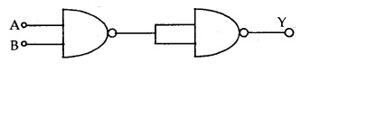
(a) AND gate
(b) OR gate
(c) NOT gate
(d) NAND
gate
Answer
Answer: (a) AND gate
Question 13.
Which of the following gates corresponds to the truth table
given here: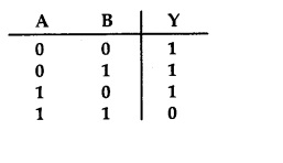
(a) NAND
(b) OR
(c) NOR
(d) AND
Answer
Answer: (a) NAND
Question 14.
The conductivity of semiconductors like Ge and Si:
(a)
increases when it is doped with pentavalent impurity.
(b) increases when it
is doped with trivalent impurity.
(c) increases when it is doped with
pentavalent or trivalent impurity.
(d) none
Answer
Answer: (c) increases when it is doped with pentavalent or trivalent impurity.
Question 15.
In which case is the junction diode forward biased.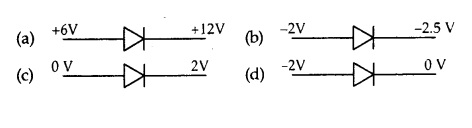
Answer
Answer: (b)
Question 16.
Assuming that the junction diode is ideal, the current in the
arrangement shown here is:![]()
(a) 2 mA
(b) 30 mA
(c) 20
mA
(d) 10 mA
Answer
Answer: (c) 20 mA
Question 17.
An oscillator is an amplifier with:
(a) a large gain
(b) Negative feedback
(c) positive feedback
(d) no
feedback
Answer
Answer: (c) positive feedback
Question 18.
How many AND gates are required to form, NAND gate?
(a)
0
(b) 1
(c) 2
(d) 4
Answer
Answer: (b) 1
Question 19.
Which of following statements is not true?
(a) Resistance
of an intrinsic semiconductor decreases with increase in temperature.
(b)
Doping pure Si with trivalent impurities gives p-type semiconductor.
(c) The
majority carriers in n-type semiconductor are holes.
(d) A p-n junction can
act as semiconductor diode.
Answer
Answer: (c) The majority carriers in n-type semiconductor are holes.
Question 20.
For a transistor, current amplification factor is 0.8. The
transistor is changed to common emitter configuration. For a change of 6 mA in
base current. Change in collector current is
(a) 4.8 mA
(b) 6 mA
(b) 8
mA
(d) 24 mA
Answer
Answer: (d) 24 mA
Question 21.
A truth table is given below. Which of the following has this
type of truth table?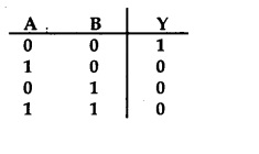
(a) XOR gate
(b) NOR gate
(b) AND gate
(d) OR gate
Answer
Answer: (b) NOR gate
Question 22.
Bonds in a semiconductor :
(a) trivalent
(b)
covalent
(c) bivalent
(d) monovalent
Answer
Answer: (b) covalent
Question 23.
Number of electrons in the valence shell of a semiconductor
is:
(a) 1
(b) 2
(c) 3
(d) 4
Answer
Answer: (d) 4
Question 24.
Semiconductors of both p-type and n-type are produced by:
(a) ionic solids
(b) covalent solids
(c) metallic solids
(d) molecular
solids
Answer
Answer: (b) covalent solids
Question 25.
With fall of temperature, the forbidden energy gap of a
semiconductor
(a) increases
(b) decreases
(c) sometimes increases and
sometimes decreases
(d) remains unchanged
Answer
Answer: (d) remains unchanged
Question 26.
In a p-type semiconductor, current conduction is by:
(a)
atoms
(b) holes
(c) electrons
(d) protons
Answer
Answer: (b) holes
Question 27.
The relation between number of free electrons (n) in a
semiconductor and temperature (T) is given by:
(a) n ∝ T
(b) n ∝ T²
(c)
n ∝ T1/2
(d) n ∝ T3/2
Answer
Answer: (d) n ∝ T3/2
Question 28.
In reverse biasing:
(a) large amount of current flows
(b) no current flows
(c) potential barrier across junction increases
(d)
depletion layer resistance increases
Answer
Answer: (c) potential barrier across junction increases
Question 29.
Main function of a transistor is to :
(a) rectify
(b)
simplify
(c) amplify
(d) all the above
Answer
Answer: (c) amplify
Question 30.
To obtain p-type silicon semiconductor, we need to dope pure
silicon with:
(a) aluminium
(b) phosphorus
(c) oxygen
(d)germanium
Answer
Answer: (a) aluminium
Question 31.
On applying reverse bias to a junction diode, it:
(a)
lowers the potential barrier
(b) raise the potential barrier
(c) increases
the majority carrier current
(d) increases the minority carrier
current
Answer
Answer: (b) raise the potential barrier
Question 32.
For germanium crystal, the forbidden energy gap in joules
(a) 1.216 × 10⁻¹⁹
(b) 1.76 × 10⁻¹⁹
(c) 1.6 ×
10-19
(d) zero
Answer
Answer: (a) 1.216 × 10⁻¹⁹
Question 33.
To obtain electrons as majority charge carriers in a
semiconductors the impurity mixed is:
(a) monovalent
(b) divalent
(c)
trivalent
(d) pentavalent
Answer
Answer: (b) divalent
Question 34.
In the middle of the depletion layer of a reverse biased p-n
junction, the:
(a) electric field is zero
(b) potential is maximum
(c)
electric field is maximum
(d) potential zero.
Answer
Answer: (d) potential zero.
Question 35.
In a common base amplifier the phase difference between the
input signal voltage and output voltage is :
(a) π/2
(b) 0
(c) π/4
(d) π
Answer
Answer: (b) 0
Question 36.
Energy bands in solids are a consequence of:
(a) Ohm’s
Law
(b) Pauli’s exclusion principle
(c) Bohr’s theory
(d) Heisenberg’s
uncertainty principle
Answer
Answer: (b) Pauli’s exclusion principle
Question 37.
In semi conductor which are responsible for conduction:
(a) only electron
(b) electron and hole both
(c) only hole
(d) None of
these
Answer
Answer: (b) electron and hole both
Question 38.
In binary system III represents:
(a) 1
(b) 3
(c)
7
(d) 100
Answer
Answer: (c) 7
Question 39.
On heating, resistance of semiconductors:
(a)
decreases
(b) increases
(c) remains same
(d) first increases then
decreases
Answer
Answer: (a) decreases
Question 40.
p-n junction diode can be used as:
(a) amplifier
(b)
oscillator
(c) detector
(d) modulator
Answer
Answer: (c) detector
Question 41.
In intrinsic semiconductor at room temperature, the number of
electrons and holes are:
(a) equal
(b) unequal
(c) infinite
(d)
zero
Answer
Answer: (a) equal
Question 42.
In full wave rectifier, input a.c. current has a frequency v.
The output frequency of current is :
(a) V/2
(b) V
(c) 2V
(d)
None
Answer
Answer: (c) 2V
Question 43.
Winch of the following gate is not an universal gate?
(a)
OR
(b) NOT
(c) AND
(d) NAND
Answer
Answer: (d) NAND
Question 44.
Zener diode is used for:
(a) producing oscillations in a
oscillator
(b) amplification
(c) stabilisation
(d)
rectification
Answer
Answer: (c) stabilisation
Question 45.
In semi conductor, at room temperature :
(a) the valence
bond is partially empty and the conduction band is partially filled
(b) the
valence band is completely filled and the conduction band is partially
filled
(c) the valence band is completely filled
(d) the conduction band
is completely empty
Answer
Answer: (a) the valence bond is partially empty and the conduction band is partially filled
Question 46.
Crystal diode is:
(a) amplifying device
(b) fluctuating
device
(c) non-linear device
(d) linear device
Answer
Answer: (c) non-linear device
Question 47.
The part of a transistor which is heavily doped to produce a
large number of majority carriers is :
(a) base
(b) emitter
(c)
collector
(d) None of these
Answer
Answer: (b) emitter
Question 48.
A p-type semiconductor is:
(a) negatively charged
(b)
positively charged
(c) uncharged
(d) None of
these
Answer
Answer: (c) uncharged
Question 49.
The material most commonly used to manufacture electronic
solid state devices is :
(a) copper
(b) silicon
(c) germanium
(d)
aluminium
Answer
Answer: (b) silicon
Question 50.
What is the number of possible crystal systems?
(a) 5
(b) 7
(c) 14
(d) 16
Answer
Answer: (b) 7
Fill in the Blanks
Question 1.
…………………. is called as junction in p-n junction
diode.
Answer
Answer: The surface of contact of p-type and n-type crystal.
Question 2.
The thickness of the depletion layer is of the order of
………………….
Answer
Answer: 1 µm = 10-6 m.
Question 3.
The potential barrier for S1 is about …………………. and
the electric field across the junction is about
………………….
Answer
Answer: 0.7V, 7 × 10³Vm-1
Question 4.
The width of the depletion layer and the potential barrier
across the junction …………………. due to reverse biasing.
Answer
Answer: increases.
Question 5.
The direction of conventional current in a p-n junction is
from …………………. when it is forward biased.
Answer
Answer: p to n region.
Question 6.
The zener voltage can have value from …………………. to ………………….
volts.
Answer
Answer: 1V, several hundred.
Question 7.
The arrow in the symbol of a transistor shows the direction
………………….
Answer
Answer: Conventional current or hole current.
Question 8.
Below knee voltage, the variation of current in the p-n
junction is …………………. and above it, it is ………………….
Answer
Answer: non-linear, linear.
Question 9.
Various components such as resistors, inductors, capacitors,
transistors, diodes and logic-gates etc. are grown over one
………………….
Answer
Answer: Semiconductor chip
Question 10.
…………………. is the most developing area where semiconductors are
used.
Answer
Answer: Computer
Question 11.
1 and 0 are called ………………….
Answer
Answer: bits.
Question 12.
The connection between logic and mathematics was realised by
…………………. and the algebra developed by him based on 0 and 1 is called
………………….
Answer
Answer: Boole, Boolean Algebra.
Question 13.
When a p-n junction is forward biased, then the motion of
charge carriers across the barrier is due to …………………. and when it is reversed
biased, then the motion of charge carriers is due to
………………….
Answer
Answer: diffusion, drift.
Question 14.
Digital circuits can be obtained by repetitive use of
…………………. gates and are called digital building
blocks.
Answer
Answer: NAND and NOR
Question 15.
In a digital circuit, the diodes and transistors are operated
by a 5V supply. The states 1 and 0 will correspond to …………………. V and …………………. V
respectively.
Answer
Answer: 5, 0
Question 16.
In insulator, the valence elctrons form a band that is
………………….
Answer
Answer: valence band which is filled completely.
Question 17.
In the band structure of an intrinsic semiconductor is
located ………………….
Answer
Answer: midway between the valence band and the conduction band.
Question 18.
The region near the junction of pn—diode where there are no
charge carriers is called ………………….
Answer
Answer: depletion region
Question 19.
A small impurity is added to Ge to get a p-type semiconductor
and this impurity is called ………………….
Answer
Answer: trivalent.
Question 20.
The Boolean expression for AND gate is
………………….
Answer
Answer: y = A.B
Question 21.
The current gain of common emitter transistor amplifier is
…………………. than one and …………………. one for common base
amplifier.
Answer
Answer: more, less.