Semiconductor Electronics, Materials, Devices and Simple Circuits
Class 12th Physics Chapter Important Questions
Class 12 Physics Chapter 14 Important Extra Questions Semiconductor Electronics: Materials, Devices and Simple Circuits
Very Short Answer Type
Question 1.
State the reason, why GaAs is most commonly used in making of
a solar cell. (All India 2008)
Answer:
GaAs is most commonly used in
making of a solar cell because :
(i) It has high optical absorption (~ 104
cm-1) .
(ii) It has high electrical conductivity.
Question 2.
Why should a photodiode be operated at a reverse bias? (All
India 2008)
Answer:
As fractional change in minority charge carriers is
more than the fractional change in majority charge carriers, the variation in
reverse saturation current is more prominent.
Question 3.
Give the logic symbol of NOR gate. (All India 2009)
Answer: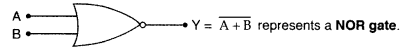
Question 4.
Give the logic symbol of NAND gate. (All India 2009)
Answer: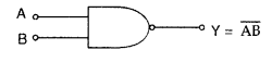
Question 5.
Give the logic symbol of AND gate. (All India 2009)
Answer: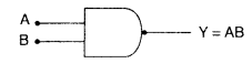
Question 6.
In a transistor, doping level in base is increased slightly.
How will it affect
(i) collector current and
(ii) base current? (Delhi
2011)
Answer:
Increasing base doping level will decrease base resistance
and hence increasing base current, which results in a decrease in collector
current.
Question 7.
What happens to the width of depletion layer of a p-n junction
when it is
(i) forward biased,
(ii) reverse biased? (Delhi 2011)
Answer:
(i) In forward biased, the width of depletion layer of a p-n junction
decreases.
(ii) In reverse biased, the width of depletion layer of a p-n
junction increases
Question 8.
What is the difference between an H-type and a p-type
intrinsic semiconductor? (Comptt. Delhi 2008)
Answer:
Question 9.
The figure shows the V-I characteristic of a semi conductor
device. Identify this device. Explain briefly, using the necessary circuit
diagram, how this device is used as a voltage regulator. (Comptt. Delhi
2011)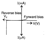
Answer:
(i) The semiconductor diode used is a Zener
diode.
(iii) Zener diode as a voltage regulator
Principle : When
a zener diode is operated in the reverse breakdown region, the voltage across it
remains practically constant (equal to the breakdown voltage Vz) for a large
change in the reverse current. If the input voltage increases, the current
through RS and zener diode also increases. This increases the voltage
drop across RS without any change in the voltage across the zener
diode. This is because in the breakdown region, zener voltage remains constant
even though the current through the zener diode changes. Similarly, if the input
voltage decreases, the voltage across RS decreases without any change
in the voltage across the zener diode. Thus any increase/decrease of the input
voltage results in increase/ decrease of the voltage drop across RS
without any change in voltage across zener diode. Hence the zener diode acts as
a voltage regulator.
Question 10.
How does the depletion region of a p-n junction diode get
affected under reverse bias? (Comptt. Delhi 2011)
Answer:
Depletion region
widens under reverse bias.
Question 11.
How does the width of depletion region of a p-n junction
diode change under forward bias?
(Comptt. Delhi 2011)
Answer:
The width
of depletion region of a p-n junction
Question 12.
The graph shown in the figure represents a plot of current
versus voltage for a given semi-conductor. Identify the region, if any, over
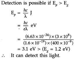
which the semi-conductor has a negative resistance.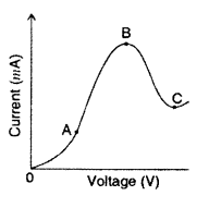
Answer:
Between the region B and C, the semiconductor has
a negative resistance.
Question 13.
Write the truth table for a NAND gate as shown in the figure.
(Comptt. All India 2013)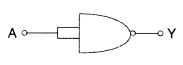
Answer:
Truth table for NAND gate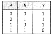
Question 14.
What is the function of a photodiode? (Comptt. All India
2013)
Answer:
A photodiode is a special purpose p-n junction diode
fabricated with a transparent window to allow light to fall on diode. It is
operated under reverse bias.
Question 15.
Write the truth table for a NOT gate connectedA as shown in
the figure. (Comptt. All India 2013)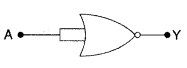
Answer:
Truth Table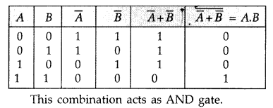
Question 16.
Write the truth table of a two point input NAND gate.
(Comptt. All India 2013)
Answer: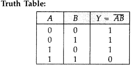
Question 17.
Show variation of resistivity of Si with temperature in a
graph. (Delhi 2014)
Answer: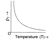
Question 18.
Plot a graph showing variation of current versus voltage for
the material GaAs. (Delhi 2014)
Answer:
A Graph showing variation of
current versus voltage for GaAs
Question 19.
Draw the logic symbol of NAND gate and give its Truth Table.
(Comptt. All India 2015)
Answer: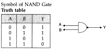
Question 20.
Identify the logic gate whose output equals 1 when both of
its inputs are 0 each. (Comptt. Delhi 2015)
Answer:
NAND gate or NOR
gate.
Question 21.
Name the junction diode whose I-V characteristics are drawn
below: (Delhi 2015)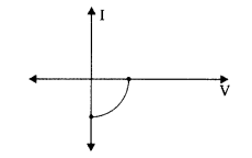
Answer:
Solar cell
Question 22.
Draw the energy band diagram for a p-type semiconductor.
Answer:
The energy level diagram is shown below.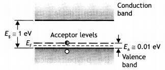
Question 23.
Draw the voltage-current characteristic of a p-n junction diode
in forwarding bias and reverse bias.
Answer:
The characteristics are as
shown.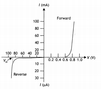
Question 24.
Draw the voltage-current characteristic for a Zener diode.
Answer:
The V-l characteristic of the Zener diode is as shown.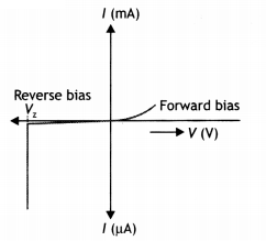
Question 25.
Draw the energy band diagram for n-type semiconductor.
Answer:
The diagram is as shown.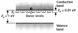
Question 26.
An ac input signal of frequency 60 Hz is rectified by an
(i)
Half wave and an
Answer:
The output frequency remains the same in a
half-wave rectifier, i.e. 60 Hz.
(ii) Full-wave rectifier. Write the output frequency in each case.
Answer:
The output frequency becomes twice the input frequency in the case of
the full-wave rectifier, i.e. 120 Hz.
Question 27.
Give the ratio of the number of holes and the number of
conduction electrons in an intrinsic semiconductor.
Answer:
The ratio is
one.
Question 28.
What is the depletion region in a p-n junction?
Answer:
It is a thin layer between p and n sections of the p-n junction which is devoid
of free electrons and holes.
Question 28 a.
Name an impurity which when added to pure silicon makes it
a
(i) p-type semiconductor
Answer:
Boron, aluminum, etc.
(ii) n-type semiconductor.
Answer:
Phosphorous, antimony, etc.
Question 29.
Which type of biasing gives a semiconductor diode very high
resistance?
Answer:
Reverse biasing.
Question 30.
Identify the biasing in the figure given below.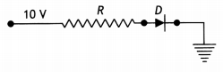
Answer:
Forward biasing.
Question 31.
Draw the circuit symbol of (a) photodiode, and (b)
light-emitting diode.
Answer:
The circuit symbols are as shown
below.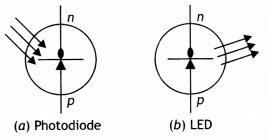
Question 32.
What is the function of a photodiode? (CBSE AI 2013C)
Answer:
It functions as a detector of optical signals.
Question 33.
When a p-n junction diode is forward biased, how will its
barrier potential be affected? (CBSEAI 2019)
Answer:
Potential barrier
decreases in forwarding bias.
Question 34.
Name the junction diode whose l-V characteristics are drawn
below: (CBSE Delhi 2017)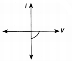
Answer:
Solar cell.
Question 35.
How does the width of the depletion region of a p-n junction
vary if the reverse bias applied to it decreases?
Answer:
With the
increase in the reverse bias, the depletion layer increases.
Question 36.
How does the width of the depletion region of a p-n junction
vary if the reverse bias applied to it decreases?
Answer:
If the reverse
bias decreases, the width of the depletion layer also decreases.
Question 37.
Why is the conductivity of n-type semiconductors greater than
that of p-type semiconductors even when both of these have the same level of
doping?
Answer:
It is because in n-type the majority carriers are
electrons, whereas in p-type they are holes. Electrons have greater mobility
than holes.
Question 38.
How does the conductance of a semiconducting material change
with rising in temperature?
Answer:
Increases with an increase in
temperature.
Question 39.
How is a sample of an n-type semiconductor electrically
neutral though it has an excess of negative charge carriers?
Answer:
It is
because it contains an equal number of electrons and protons and is made by
doping with a neutral impurity.
Question 40.
How is the bandgap, Eg, of a photodiode related to the
maximum wavelength, λm, that can be detected by it?
Answer:
Eg = \(\frac{h c}{\lambda_{m}}\)
Question 41.
Zener diodes have higher dopant densities as compared to
ordinary p-n junction diodes. How does it affect the
(i) Width of the
depletion layer
Answer:
Junction width will be small and
(ii) Junction field?
Answer:
The junction field will be high.
Question 42.
Can the potential barrier across a p-n junction be measured
by simply connecting a voltmeter across the junction? (NCERT Exemplar)
Answer:
No, because the voltmeter must have a resistance very high compared
to the junction resistance, the latter being nearly infinite.
Short Answer Type
Question 1.
Draw a labeled circuit diagram of a full-wave rectifier using
a p-n junction.
Answer:
The diagram is as shown.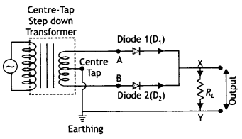
Question 2.
What is a solar cell? How does it work? Give one of its uses.
Answer:
It is a p-n junction used to convert light into electrical energy. In
such a diode, one region either the p-type or the n-type is made so thin that
light falling on the diode is not absorbed appreciably before reaching the
junction. The thin region in the solar cell is called the emitter and the other
is called the base. The magnitude of current depends upon the intensity of light
reaching the junction. A solar cell can be used to charge storage batteries
during the daytime, which can be used during the night.
These are used as power supplies for satellites and space vehicles.
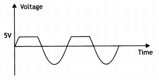
Question 3.
Draw the output signal in a p-n junction diode when a square
input signal of 10 V as shown in the figure is applied across it. (CBSE AI
2019)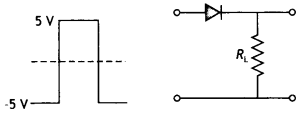
Answer:
The diode will conduct only when it is forward biased. Therefore,
till the input voltage is + 5 V, we will get an output across R, accordingly the
output waveform shown in the figure.
Question 4.
The following diagrams, indicate which of the diodes are
forward biased and which are reverse biased.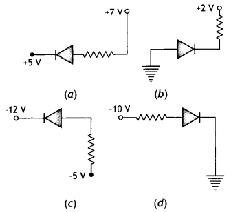
Answer:
(a) Forward biased.
(b) Reverse biased.
(c) Forward biased,
(d) Reverse biased.
Question 5.
Mention the important considerations required while
fabricating a p-n junction diode to be used as Light-Emitting Diode (LED). What
should be the order of bandgap of an LED if it is required to emit light in the
visible range? (CBSE Delhi 2013)
Answer:
The important considerations
are
- It should be heavily doped.
- The diode should be encapsulated with a transparent cover so that emitted light can come out.
The semiconductor used for the fabrication of visible LEDs must at least have a bandgap of 1.8 eV.
Question 6.
In the given circuit diagram shown below, two p-n junction
diodes D1 and D2 are connected with a resistance R and a
dc battery E as shown. Redraw the diagram and indicate the direction of flow of
appreciable current in the circuit. Justify your answer.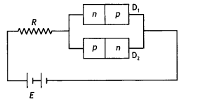
Answer:
The redrawn diagram showing the flow of appreciable current is shown
below.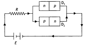
Here diode D2 is forward biased, hence it conducts. Therefore
appreciable current will pass through it. However, diode 0, is reverse biased,
hence negligible current will flow through it.
Question 7.
The diagram below shows a piece of pure semiconductor S in
series with a variable resistor R and a source of constant voltage V. Would you
increase or decrease the value of R to keep the reading of ammeter (A) constant
when semiconductor S is heated? Give reason.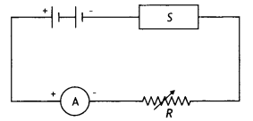
Answer:
When a semiconductor is heated, its resistance decreases. As a
result, the total resistance of the circuit will decrease. In order to maintain
constant current flow, the total resistance of the circuit must remain constant.
Hence, the external resistance has to be increased to compensate for the
decrease of resistance of the semiconductor.
Question 8.
Distinguish between an intrinsic semiconductor and p-type
semiconductor. Give reason, why, a p-type semiconductor crystal is electrically
neutral although nh >> ne? (Delhi 2008)
Answer: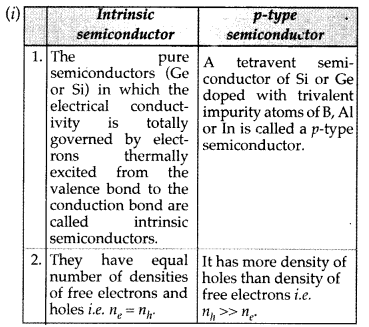
(ii) In a p-type semiconductor, the trivalent impurity atom
shares its three valence electrons with the three tetravalent host atoms while
the fourth bond remains unbounded. The impurity atom as a whole is electrical
neutral. Hence the p-type semiconductor is also neutral.
Question 9.
The given inputs A, B are fed to a 2-input NAND gate. Draw
the output wave form of the gate.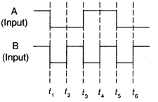
Answer: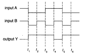
Question 10.
Draw the output wave form at X, using the given inputs A, B
for the logic circuit shown below. Also identify the gate. (Delhi 2008)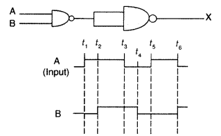
Answer: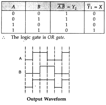
Question 11.
If the output of a 2 input NOR gate is fed as both inputs A
and B to another NOR gate, write down a truth table to find the final output,
for all combinations of A, B. (Delhi 2008)
Answer:
The truth table
is: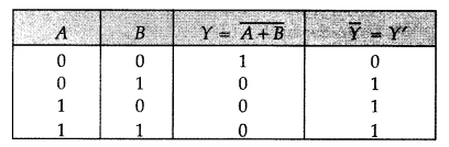
Question 12.
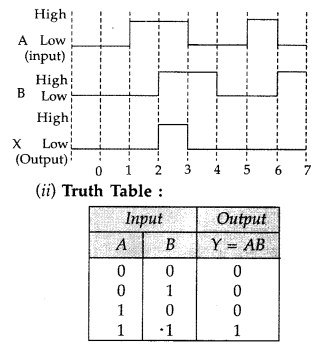
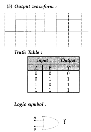
The following figure shows the input waveforms (A, B) and the
output waveform (Y) of gate. Identify the gate, write its truth table and draw
its logic symbol. (Delhi 2009)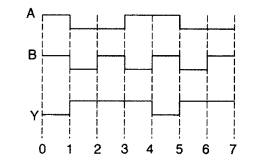
Answer:
Question 13.
The output of a 2-input AND gate is fed to a NOT gate. Give
the name of the combination and its logic symbol. Write down its truth table.
(Delhi 2009)
Answer:
Name : NAND gate.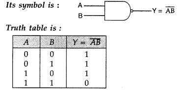
Question 14.
(i) Sketch the output waveform from an AND gate for the
inputs A and B shown in the figure.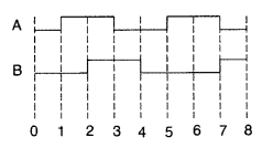
(ii) If the output of the above AND gate is fed to a NOT
gate, name the gate of the combination so formed. (Delhi 2009)
Answer: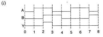
(ii) If this output of AND gate is fed to a NOT gate, the
result will be a NAND gate.
Question 15.
Draw the circuit diagram of an illuminated photodiode in
reverse bias. How is photodiode used to measure light intensity? (Delhi
2010)
Answer:
A measurement of the change in the reverse. saturation
current on illumination can give the values of light intensity because
photocurrent is pro-portional to incident light intensity.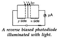
Question 16.
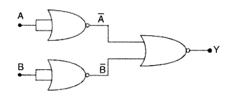
(i) Identify the logic gates marked P and Q in the given
logic circuit.
(ii) Write down the output at X for the inputs A = 0, B = 0
and A = 1, B = 1. (All India 2010)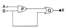
Answer:
(i) P is NAND gate and Q is OR gate.
Question 17.
(i) Identify the logic gates A marked P and Q B in the given
logic circuit.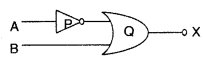
(ii) Write down the output at X for the inputs A = 0, B = 0
and A = 1, B = 1. (All India 2010)
Answer:
(i) P is NOT gate
Q is OR
gate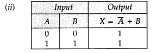
Question 18.
Draw the output wave form at X, using the given inputs A and
B for the logic circuit shown below. Also, identify the logic operation
performed by this circuit. (Delhi 2011)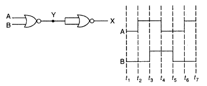
Answer:
Question 19.
Name the semiconductor device that can be used to regulate an
unregulated dc power supply. With the help of I-V characteristics of this
device, explain its working principle. (Delhi 2011)
Answer:
Name : Zener
diode is used to regulate an unregulated dc power supply.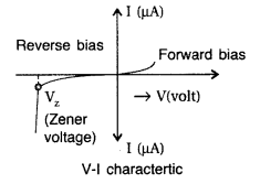
Working principle : When a zener diode is operated in the
reverse break down region, the voltage across it remains practically constant
(equal to the break down voltage V-I) for a large change in the reverse
current.
Question 20.
Draw the transfer characteristic curve of a base biased
transistor in CE configuration. Explain clearly how the active region of the VD
versus V, curve in a transistor is used as an amplifier. (Delhi 2011)
Answer:
For using the transistor as an amplifier we will use the active
region of the V0 vs. V, curve. The slope of the linear part of the curve
represents the rate of change of the output with input. It is negative, that is
why as input voltage of the CE amplifier increases its output voltage decreases
and the output is said to be out of phase with input.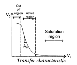
Question 21.
Draw the output waveform at X, using the given inputs A and B
for the logic circuit shown below. Also, identify the logic operation performed
by this circuit.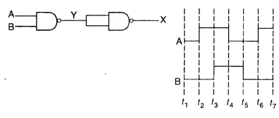
Answer: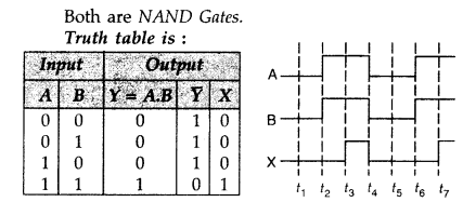
Question 22.
How is forward biasing different from reverse biasing in a pn
junction diode? (Delhi 2011)
Answer:
Forward biasing : If the positive
terminal of a battery is connected to a p-side and the negative terminal to the
72-side, then the p-n junction is said to be forward biased. Here the applied
voltage V opposes the barrier voltage VB. As a result of this
- the effective resistance across the p-n junction decreases.
- the diffusion of electrons and holes into the depletion layer which decreases its width.
Reverse biasing : If the positive terminal of a battery is connected to the
72-side and negative terminal to the p-side, then the p-n junction is said to be
reverse biased.
The applied voltage V and the barrier potential VB
are in the same direction. As a result of this
- the resistance of the p-n junction becomes very large.
- the majority charge carriers move away from the junction, increasing the width of the depletion layer.
Question 23.
Explain how a depletion region is formed in a junction diode.
(Delhi 2011)
Answer:
As soon as a p-n junction is formed, the majority
charge carriers begin to diffuse from the regions of higher concentration to the
regions of lower concentrations. Thus the electrons from the n-region diffuse
into the p-region and where they combine with the holes and get neutralised.
Similarly, the holes from the p-region diffuse into the n-region where they
combine with the electrons and get neutralised. This process is called
electron-hole recombination.
The p-region near the junction is left with immobile -ve ions
and n-region near the junction is left with +ve ions as shown in the figure. The
small region in the vicinity of the junction which is depleted of free charge
carriers and has only immobile ions is called the depletion layer. In the
depletion region, a potential difference VB is created, called potential barrier
as it creates an electric field which opposes the further diffusion of electrons
and holes.
(i) In forward biased, the width of depletion region is
decreased.
(ii) In reverse biased, the width of depletion region is
increased.
Question 24.
Write the truth table for the logic circuit shown below and
identify the logic operation performed by this circuit.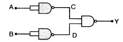
Answer: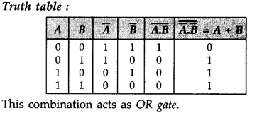
Question 25.
The current in the forward bias is known to be more (~mA)
than the current in the reverse bias (~µA). What is the reason, then, to operate
the photodiode in reverse bias? (Delhi 2012)
Answer:
The fractional
increase in majority carriers is much less than the fractional increase in
minority carriers. Consequently, the fractional change due to the photo-effects
on the minority carrier dominated reverse bias current is more easily measurable
than the fractional change in the majority carrier dominated forward bias
current.
Question 26.
Describe briefly with the help of a circuit diagram, how the
flow of current carriers in a p-n-p transistor is regulated with emitter-base
junction forward biased and base-collector junction reverse biased. (All India
2012)
Answer:
In a p-n-p transitor, the heavily doped emitter which is
p-type has a majority charge carrier of holes. These holes when move towards
21-type base get neutralized by e– in base. The majority carriers
enter the base region in large numbers. As the base is thin and lightly doped,
the majority carriers (holes) swamp the small number of electrons there and as
the collector is reverse biased, these holes can easily cross the junction and
enter the collector.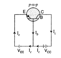
Question 27.
(a) Why are Si and GaAs preferred materials for fabrication
in solar cells?
(b) Draw V-I characteristic of solar cell and mention its
significance.(Comptt. All India 2012)
Answer:
(a) The important criteria
for the fabrication of a material for solar cell fabrication are :
(i) Band
gap of the order of 1.0 eV to 1.8 eV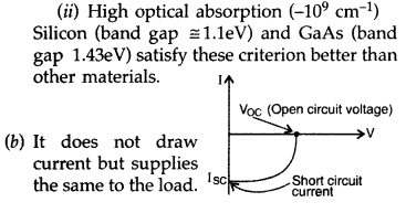
Question 28.
In the given circuit diagram, a voltmeter ‘V’ is connected
across a lamp ‘L’. How would
(i) the brightness of the lamp and
(ii)
voltmeter reading ‘V’ be affected, if the value of resistance ‘R’ is decreased?
Justify your answer. (Delhi 2012)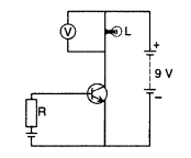
Answer:
When the value of R is decreased, forward biasing
of emitter-base junction increases. As a result of this, the emitter current and
hence the collector current increases. Therefore :
(i) The bulb glows more
brightly.
(ii) The reading of voltmeter is increased.
Question 29.
Explain, with the help of a circuit diagram, the working of a
photo-diode. Write briefly how it is used to detect the optical signals. (Delhi
2013)
Answer:
Working of a photo-diode: Its working is based on photo
conduction from light. The conductivity of p-n junction photodiode increases
with the increase in intensity of light falling in it.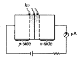
When visible light of energy greater than forbidden energy
gap (i.e. hv > Eg) is incident on a reverse biased p-n junction
photodiode, additional electron-hole pairs are created in the depletion layer
(or near the junction) due to the absorption of photons. The charge carriers
will be separated by the junction field and made to flow across the junction,
creating reverse current across the junction. The value of reverse saturation
current increases with increase in the intensity of incident light. It is found
that the reverse saturation current through the photodiode varies almost
linearly with the light flux.
When the photodiode is reverse biased then a certain current exits in the circuit even when no light is incident on the p-n junction of photodiode. This current is called dark current. A photodiode can turn its current ON and OFF in nanoseconds. Hence it can be used to detect the optical signals.
Question 30.
Mention the important considerations required while
fabricating a p-n junction diode to be used as a Light Emitting Diode (LED).
What should be the order of band gap of an LED if it is required to emit light
in the visible range? (Delhi 2013)
Answer:
The important considerations
required while fabricating a p-n junction diode to be used as a Light Emitting
Diode (LED) are :
(i) The Light Emitting efficiency is maximum.
(ii) The
reverse breakdown voltage of LEDs are very low. Care should be taken that high
reverse voltages do not appear across them.
(iii) The semiconductor used for
fabrication of visible, LEDs must have a band gap of 1.8 eV (spectral range of
visible light is from about 0.4 µm to 0.7 µm i.e. from about 3 eV to 1.8
eV).
Question 31.
Draw typical output characteristics of an n-p-n transistor in
CE configuration. Show how these characteristics can be used to determine output
resistance. (All India 2013)
Answer:
Typical output characteristic curves
: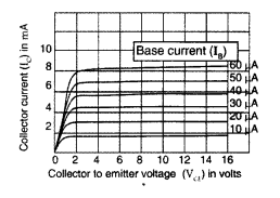
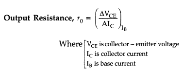
The reciprocal of the slope of the linear part of the output
characteristic gives the value of output resistance (r0). The output
resistance of the transistor is mainly controlled by the base-collector
junction. The high magnitude of the output resistance (of the order of 100 KΩ)
is due to the reverse biased state of this diode. This also explains why the
resistance at the initial part of the characteristic, when the transistor is in
saturation, is very low.
Question 32.
In the circuit shown in the figure, identify the equivalent
gate of the circuit and make its truth table.(All India 2013)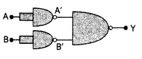
Answer:
The equivalent gate is OR.
Truth table
:
Question 33.
In the circuit shown in the figure, identify the equivalent
gate of the circuit and make its truth table.
(All India 2013)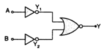
Answer:
AND Gate
Truth table: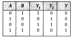
Question 34.
In the circuit shown in the figure, identify the equivalent
gate of the circuit and make its truth table. (All India 2013)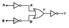
Answer: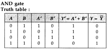
Question 35.
Assuming that the two diodes Dj and D2 used in the electric
circuit shown in the figure are ideal, find out the value of the current flowing
through 1Ω resistor. (Comptt. Delhi 2013)
Answer:
Since the diodes used
are ideal, the diode Dj in forward bias will conduct the current in forward
direction, while diode D2 in reverse bias will not allow any current
to flow.
As such, 2Ωwith D1 and 1Ω are in series, the net
resistance of the circuit will be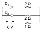
Hence the value of the current flowing through 1Ω resistor =
2A
Question 36.
Assuming that the two diodes D1 and D2
used in the electric circuit shown in the figure are ideal, find out the value
of the current flowing through 2.5 Ω resistor. (Comptt. Delhi 2013)
Answer: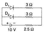
Value of the current flowing through 2.5 Ω resistor = 2.5
A
Question 37.
Assuming that the two diodes D1 and D2
used in the electric circuit shown in the figure are ideal, find out the value
of the current flowing through 2 Ω resistor. (Comptt. Delhi 2013)
Answer:
D1 will conduct current while D2 will not allow Hence R =
3Ω + 2Ω = 5Ω As such, 2Ω with D1 and 2Ω are in series, the net
resistance of the circuit will be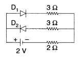
∴ Value of the current flowing through 2Ω resistor = 0.4A
Question 38.
Write the truth table for the combination of the gates shown.
Name the gates used. (Delhi 2013)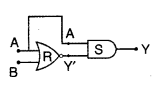
Answer:
R gate = OR
S gate = AND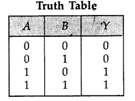
Question 39.
Identify the logic gates marked ‘P’ and ‘Q’ in the A given
circuit. Write the B truth table for the combination. (Delhi 2013)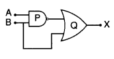
Answer:
P gate = NAND
Q gate = OR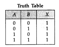
Question 40.
Explain, with the help of a circuit diagram, the working of a
p-n junction diode as a half-wave rectifier. (All India 2013)
Answer:
Rectifier. A rectifier is a circuit which converts an alternating current into
direct current.
p-n diode as a half wave rectifier. A half wave rectifier
consists of a single diode as shown in the circuit diagram. The secondary of the
transformer gives the desired a.c. voltage across A and B.
In the positive
half cycle of a.c., the voltage at A is positive, the diode is forward biased
and it conducts current.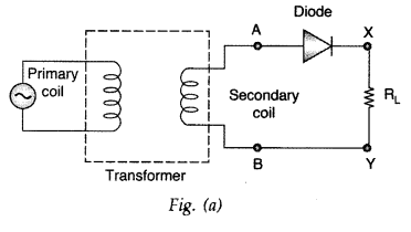
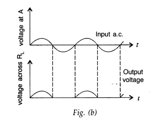
In the negative half cycle of a.c., the voltage at A is
negative, the diode is reversed biased and it does not conduct current.
Thus,
we get output across RL during positive half cycles only. The output
is unidirectional but varying
Question 41.
Draw a circuit diagram of n-p-n transistor amplifier in CE
configuration. Under what condition does the transistor act as an amplifier?
(All India 2014)
Answer: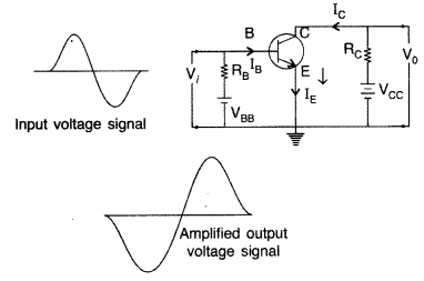
Condition: The linear portion of the active region of the
transistor is used as an amplifier.
Question 42.
The outputs of two NOT gates are fed to a NOR gate. Draw the
logic circuit of the combination of gates. Give its truth table. Identify the
gate represented by this combination. (Comptt. Delhi 2014)
Answer: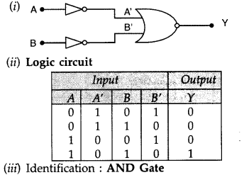
Question 43.
Name the gates ‘P’ and ‘Q’ shown in the figure of logic
circuit of logic circuit given below. Write the truth table for the combination
of the gates and identify the equivalent gate. (Comptt. Delhi)![]()
Answer:
P gate : AND
Q gate : NOT
Identification of
gate : NAND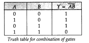
Question 44.
Name the gates ’F and ‘Q’ in the logic circuit shown in the
figure. Write the truth table for the combination of the gates and identify the
equivalent gate.![]()
Answer:
P gate : NOT
Q gate : AND
Identification of
equivalent gate : NAND
Question 45.
The input waveforms ‘A’ and ‘B’ and the output waveform ‘Y’
of a gate are shown. Name the gate it represents, write its truth table and draw
the logic symbol of this gate. (Comptt. All India 2014)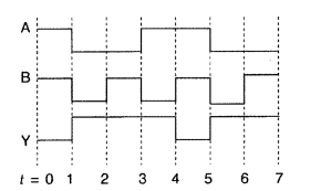
Answer: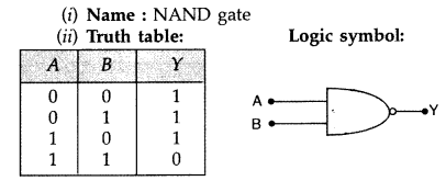
Question 46.
(a) Write the truth table for an OR gate and draw its logic
symbol.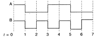
(b) The input waveforms A and B, shown here, are fed to an
AND gate. Find the output waveform. (Comptt. All India 2014)
Answer: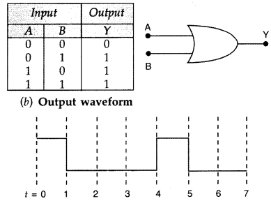
Question 47.
(i) Write the truth table for an AND gate and draw its logic
symbol.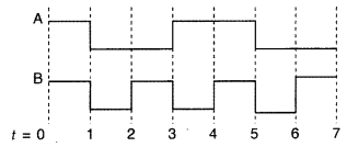
(ii) The input waveforms A and B, as shown, are fed to a NAND
gate. Find the output waveform. (Comptt. All India 2014)
Answer: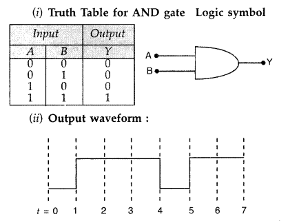
Question 48.
Distinguish between ‘intrinsic’ and ‘extrinsic’
semiconductors. (Delhi 2015)
Answer: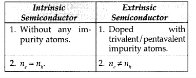
Question 49.
The following data was obtained for a given transistor
: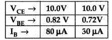
For this data, calculate the input resistance of the given
transistor. (Comptt. Delhi 2015)
Answer: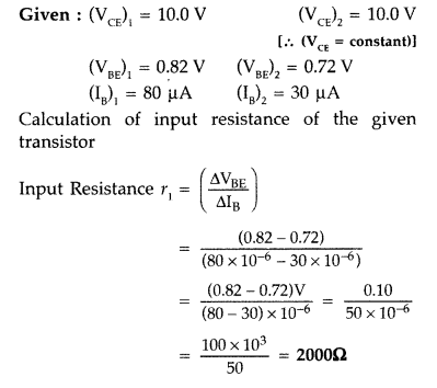
Question 50.
The figure given below shows the V-I characteristic of a
semiconductor diode.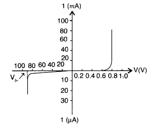
(i) Identify the semiconductor diode used.
(ii) Draw the
circuit diagram to obtain the given characteristic of this device.
(iii)
Briefly explain how this diode can be used as a voltage regulator. (Delhi
2015)
Answer:
(i) The semiconductor diode used is a Zener diode.
(iii) Zener diode as a voltage regulator
Principle : When
a zener diode is operated in the reverse breakdown region, the voltage across it
remains practically constant (equal to the breakdown voltage Vz) for a large
change in the reverse current. If the input voltage increases, the current
through RS and zener diode also increases. This increases the voltage
drop across RS without any change in the voltage across the zener
diode. This is because in the breakdown region, zener voltage remains constant
even though the current through the zener diode changes. Similarly, if the input
voltage decreases, the voltage across RS decreases without any change
in the voltage across the zener diode. Thus any increase/decrease of the input
voltage results in increase/ decrease of the voltage drop across RS
without any change in voltage across zener diode. Hence the zener diode acts as
a voltage regulator.
Question 51.
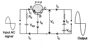
Draw the labelled circuit diagram of a common-emitter
transistor amplifier. Explain clearly how the input and output signals are in
opposite phase. (All India 2008)
Answer:
The diagram shows the circuit
diagram of a n-p-n trasistor as a CE amplifier. In this diagram it is evident
that the base-emitter junction is forward biased whereas collector emitter
junction is set to be reverse biased for an ideal operation as an amplifier. In
absence of any input a.c. signal the p.d. between collector and emitter is given
by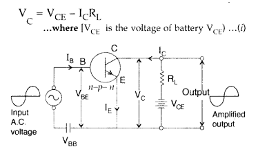
In the presence of an input a.c. signal, the forward biased
voltage increases resulting in an increase in collector current IC
during the positive half cycle, which further decreases the VC from
equation (i) Whereas IE and IC both decrease during the
negative half cycle as a result of reverse biasing of input section, the
decrease in IC increases the VC. So the change in
VC during the positive and negative half input cycle results in a
180° phase difference between input and output.
Question 52.
State briefly the underlying principle of a- transistor
oscillator. Draw a circuit diagram showing how the feedback is accomplished by
inductive coupling. Explain the oscillator action. (All India 2008)
Answer:
Principle of transistor oscillator : “Sustained a.c. signals can he
obtained from an amplifier circuit without any external input signal by giving a
positive feedback to the input circuit through inductive coupling or RC/LC
network.”
Oscillator action : In an ideal n-p-n biased transistor, when input base
emitters junction and output base collector junction are forward and reverse
biased respectively, a high collector current IC flows through the
circuit. If in circuit switch S is on, this current IC will start
flowing in the emitter circuit through the inductive coupling between coils
T1 and T2, which provides the +ve feedback output to input
and hence make IE maximum. In the absence of +ve feedback the IE thus
decreases making the circuit back to its original state. This process continues
and ocillations are produced.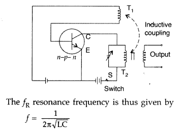
Question 53.
The inputs A and B are inverted by using two NOT gates and
their outputs are fed to the NOR gate as shown:
Analyse the action of the
gates (1) and (2) and identify the logic gate of the complete circuit so
obtained. Give its symbol and the truth table. (All India 2008)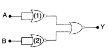
Answer: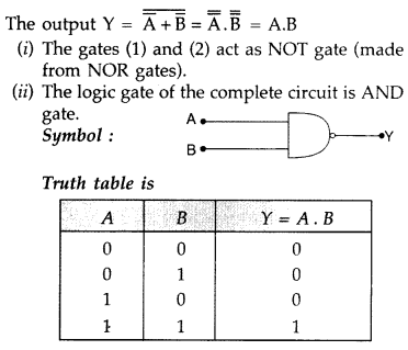
Question 54.
With the help of a suitable diagram, explain the formation of
depletion region in a p-n junction. How does its width change when the junction
is
(i) forward biased, and
(ii) reverse biased? (All India 2008)
Answer:
As soon as a p-n junction is formed, the majority charge carriers
begin to diffuse from the regions of higher concentration to the regions of
lower concentrations. Thus the electrons from the n-region diffuse into the
p-region and where they combine with the holes and get neutralised. Similarly,
the holes from the p-region diffuse into the n-region where they combine with
the electrons and get neutralised. This process is called electron-hole
recombination.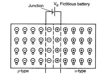
The p-region near the junction is left with immobile -ve ions
and n-region near the junction is left with +ve ions as shown in the figure. The
small region in the vicinity of the junction which is depleted of free charge
carriers and has only immobile ions is called the depletion layer. In the
depletion region, a potential difference VB is created, called potential barrier
as it creates an electric field which opposes the further diffusion of electrons
and holes.
(i) In forward biased, the width of depletion region is
decreased.
(ii) In reverse biased, the width of depletion region is
increased.
Question 55.
Give a circuit diagram of a common emitter amplifier using an
n-p-n transistor. Draw the input and output waveforms of the signal. Write the
expression for its voltage gain. (All India 2009)
Answer:
(i) (a) Common
emitter configuration of n-p-n transistor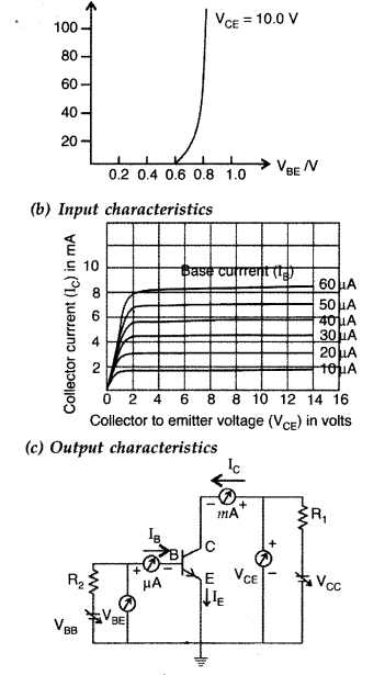
(ii) Transistor as an amplifier (C.E. configuration) : The
circuit diagram of a common emitter amplifier using n-p-n transistor is given
below :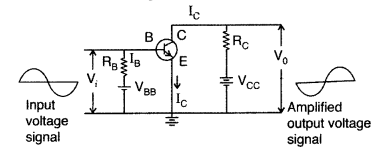
The input (base-emitter) circuit is forward biased and the
output circuit (collector- emitter) is reverse biased.
When no a.c. signal is
applied, the potential difference VCC between the collector and
emitter is given by![]()
When an a.c. signal is fed to the input circuit, the forward
bias increases during the positive half cycle of the input. This results in
increase in IC and decreases in VCC. Thus during positive
half cycle of the input, the collector becomes less positive.
During the negative half cycle of the input, the forward bias is decreased
resulting in decrease in IE and hence IC. Thus
VCC would increase making the collector more positive. Hence in a
common-emitter amplifier, the output voltage is 180° out of phase with the input
voltage.![]()
Question 56.
(i) With the help of circuit diagrams, distinguish between
forward biasing and reverse biasing of a p-n junction diode.
(ii) Draw V-I
characteristics of a p-n junction diode in
(a) forward bias,
(b) reverse
bias. (All India 2009)
Answer: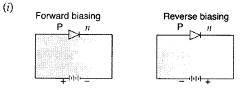
Question 57.
Explain with the help of a circuit diagram how a zener diode
works as a DC voltage regulator. Draw its I – V characteristics. (All India
2009)
Answer:
Zener diode is fabricated by heavily doping both p and
n-sides. Due to this, depletion region formed is very thin (< 10-6
n and the electric field of the junction is extremely high (~5 × 10⁶
V / m) even for a small reverse bias voltage of 5 volts. It is seen that when
the applied reverse bias voltage (V) reaches the breakdown voltage (Vz) of the
Zener diode, there is a large change in the current. After the breakdown voltage
Vz, a large change in the current can be produced by almost insignificant change
in the reverse bias voltage. In other words, Zener voltage remains constant even
though current through the Zener diode varies over a wide range. This property
of the Zener diode is used for regulating voltages so that they are constant.
Semiconductor diode as a half wave Rectifier : The junction diode D, supplies
rectified current to the band during one half of the alternating input voltage
and is always in the same direction. During the first half cycles of the
alternating input voltage, junction diodes D1 will conduct each
permitting current to flow during one half cycle whenever its p-terminal is
positive with respect to the n-terminal.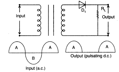
The resulting output current is a series of unidirectional
pulses with alternate gaps.
Question 58.
Draw a labelled diagram of a full wave rectifier circuit.
State its working principle. Show the input-output waveforms. (All India
2009)
Answer:
p-n junction diode as full wave rectifier
A full wave
rectifier consists of two diodes and special type of transformer known as centre
tap transformer as shown in the circuit. The secondary of transformer gives the
desired a.c. voltage across A and B.
During the positive half cycle of a.c.
input, the diode D1 is in forward bias and conducts current while
D2 is in reverse biased and does not conduct current. So we get an
output voltage across the load resistor RL.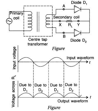
During the negative half cycle of a.c. input, the diode
D1 is in reverse biased and does not conduct current while diode
D2 in forward biased and conducts current. So we get an output
voltage across the load resistor RL.
NOTE: This is a more
efficient circuit for getting rectified voltage or current.
Question 59.
You are given a circuit below. Write its truth table. Hence,
identify the logic operation carried out by this circuit. Draw the logic symbol
of the gate it corresponds to.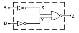
Answer: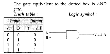
Question 60.
You are given a A circuit below. Write its truth table.
Hence, identify the B logic operation carried out by this circuit. Draw the
logic symbol of the gate it corresponds to. (All India 2011)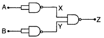
Answer:
Question 61.
You are given a circuit below. Write its truth A table.
Hence, identify the logic operation B carried out by this circuit. Draw the
logic symbol of the gate it corresponds to. (All India 2011)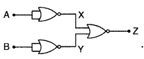
Answer: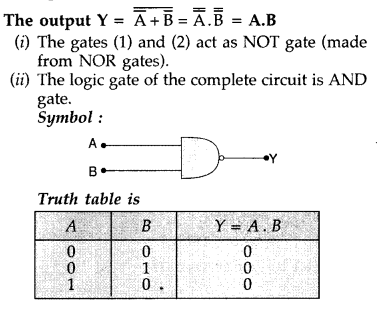
Question 62.
Draw the transfer characteristic of a base-biased transistor
in CE configuration. Mark the regions where the transistor can be used as a
switch. Explain briefly its working. (Comptt. Delhi 2011)
Answer:
Transistor as a switch. The circuit diagram of transistor as a switch is shown
in Figure 1. Transfer characteristics. The graph between V0 and
Vi is called the transfer characteristics of the base-biased
transistor, shown in Figure 2.
When the transistor is used in the cut off or saturation state, it acts as a switch.
As long as Vi is low and unable to forward bias the transistor,
then V0 is high. If Vi is high enough to drive the
transistor into saturation, then V0 is low. When the transistor is
not conducting, it is said to be switched off and when it is driven into
saturation, it is said to be switched on. This shows that a low input switches
the transistor off and a high input switches it on.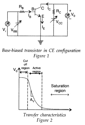
Question 63.
The figure shows the V-I characteristics of a semiconductor
device. Identify this device. Explain briefly, using the necessary circuit
diagram, how this device is used as a voltage regulator. (Comptt. Delhi
2012)
Answer:
(i) The semiconductor diode used is a Zener diode.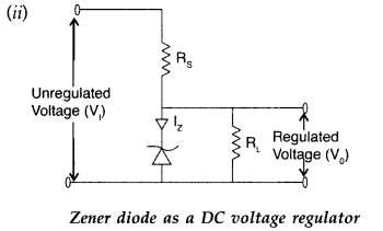
(iii) Zener diode as a voltage regulator
Principle : When
a zener diode is operated in the reverse breakdown region, the voltage across it
remains practically constant (equal to the breakdown voltage Vz) for a large
change in the reverse current. If the input voltage increases, the current
through RS and zener diode also increases. This increases the voltage
drop across RS without any change in the voltage across the zener
diode. This is because in the breakdown region, zener voltage remains constant
even though the current through the zener diode changes. Similarly, if the input
voltage decreases, the voltage across RS decreases without any change
in the voltage across the zener diode. Thus any increase/decrease of the input
voltage results in increase/ decrease of the voltage drop across RS
without any change in voltage across zener diode. Hence the zener diode acts as
a voltage regulator.
Question 64.
Output characteristics of an n-p-n transistor in CE
configuration is shown in the figure.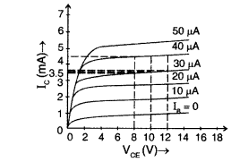
Determine
(i) dynamic output resistance
(ii) dc current
gain and
(iii) ac current gain at an operating point
VCE = 10
V, IB = 30 µA (Delhi 2012)
Answer: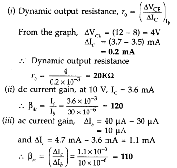
Question 65.
Draw V-I characteristics of a p-n junction diode.
Answer
the following questions, giving reasons:
(i) Why is the current under reverse
bias almost independent of the applied potential upto a critical voltage?
(ii) Why does the reverse current show a sudden increase at the critical
voltage.
Name any semiconductor device which operates under the reverse bias
in the breakdown region.
(All India 2012)
Answer:
(i) In reverse bias
of p-n junction diode the small current is due to minority carrier and hence
resistance is also very high. Increase in voltage leads to a very-very small
increase in reverse bias currents so we conclude that in reverse bias reverse
current is almost independent of applied potential upto a critical voltage
because after this critical voltage, current increases suddenly.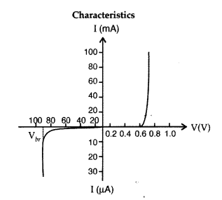
(ii) In reverse bias, reverse current through junction diode
is due to minority charge carriers. As reverse bias voltage is increased,
electric field at junction becomes significant. When reverse bias voltage
becomes equal to zener voltage, electric field strength across junction becomes
high. Electric field across junction is sufficient to pull valence electrons
from the atom on p- side and accelerate them towards n-side. The movement of
these electrons across the function account for high current which is observed
at breakdown reverse voltage. Zener diode and photo diode operate under reverse
bias.
Question 66.
Write any two distinguishing features between conductors,
semiconductors and insulators on the basis of energy band diagrams. (All India
2012)
Answer:
Distinguishing features between conductors, semiconductors
and insulators :
(i) Insulator. In insulator, the valence band is completely
filled. The conduction band is empty and forbidden energy gap is quite large. So
no electron is able to go from valence band to conduction band even if electric
field is applied. Hence electrical conduction is impossible. The solid/
substance is an insulator.
(ii) Conductors (Metals). In metals, either the
conduction band is partially filled or the conduction and valence band partly
overlap each other. If small electric field is applied across the metal, the
free electrons start moving in a direction opposite to the direction of electric
field. Hence, metal behaves as a conductor.
(iii) Semiconductors. At absolute
zero kelvin, the conduction band is empty and the valence band is filled. The
material is insulator at low temperature. However the energy gap between valence
band and conduction band is small. At room temperature, some valence electrons
acquire thermal energy and jump to conduction band where they can conduct
electricity. The holes left behind in valence band act as a positive charge
carrier.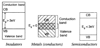
Question 67.
With what considerations in view, a photodiode is fabricated?
State its working with the help of a suitable diagram.
Even though the
current in the forward bias is known to be more than in the reverse bias, yet
the photodiode works in reverse bias. What is the reason? (Delhi 2014)
Answer:
(a) Why is photodiode fabricated?
- It is fabricated with a transparent window to allow light to fall on diode.
(b) Working of photodiode : When the
photodiode is illuminated with
photons of energy (hv > Eg) greater than the energy gap
- of the semiconductor, electron-holes pairs are generated. These get separated due to the Junction electric field (before they recombine) which produces an emf.
(c) Diagram of photodiode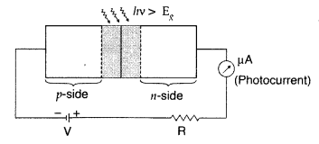
(d) Reason. It is easier to observe the change in the current, with change in light intensity, if a reverse bias is applied.
Question 68.
Draw a circuit diagram of a transistor amplifier in CE
configuration.
Define the terms :
(i) Input resistance and
(ii) Current
amplification factor. How are these determined using typical input and output
characteristics? (Delhi 2012)
Answer:
Circuit diagram of Transistor
Amplifier in CE configuration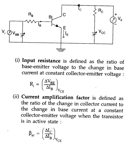
The value of input resistance is determined from the slope of
IB versus VBE plot at constant VCE.
The
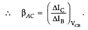
value of current amplification factor is obtained from the slope of collector
current IC versus VCE plot, using different values of
IB.
Question 69.
Identify the gates P and Q shown in A – the figure. Write B”
the truth table for the combination of the gates shown.
Name the equivalent gate representing this circuit and write
its logic symbol. (All India 2014)
Answer:
(i) P acts as AND gate; Q as
NOT gate.
(ii) Truth table for combination of gates P and Q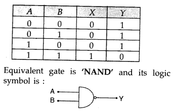
Question 70.
Draw a circuit diagram of a C.E. transistor amplifier.
Briefly explain its working and write the expression for
(i) current gain
(ii) voltage gain of the amplifier.
Answer: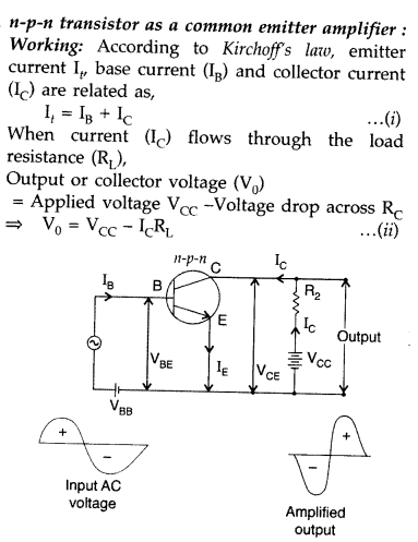
During the positive half cycle of input signal, the forward
bias of emitter-base junction increases.
Due to increased forward bias,
emitter current (IE) increases and hence according to equation (i)
collector current (IC) also increases. Therefore, the voltage drop
across RL (i.e. ICRL) increases. According to
equation (ii), the collector voltage or output voltage (V0)
decreases. Thus collector is connected to the positive terminal of the battery
(VCC)
so decrease in V0 means that the collector
voltage becomes 1 cm positive. In other words, amplified negative signal is
obtained across the output.
Similarly, during negative hay cycle, an
amplified positive signal is obtained across the output.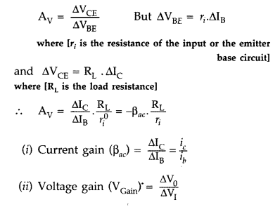
Question 71.
Distinguish between «-type and p-type semi-conductors on the
basis of energy band diagrams. Compare their conductivities at absolute zero
temperature and at room temperature. (Comptt. Delhi 2014)
Answer:
Distinction between n-type and p-type semiconductors on the basis of energy
level diagram :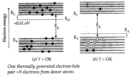
(i) In n-type semi conductors an extra energy level (called
donor energy level) is produced just below the bottom of the conduction band,
while in the p-type semiconductor, this extra energy band (called acceptor
energy level) is just above the top of the balanced band.
(ii) In n-type
semiconductors, most of the electrons come from the donor impurity while in
p-type semiconductor, the density of holes in the valence band is predominantly
due to the impurity in the extrinsic semiconductors.
(iii) At absolute zero
temperature conductivities of both types of semi-conductors will be zero.
(iv) For equal doping, an n-type semiconductor will have more conductivity than
a p-type semiconductor, at room temperature.
Question 72.
Draw the energy band diagram of
(i) n-type and
(ii)
p-type semiconductor at temperature, T > OK. In the case n-type Si
semiconductor, the donor level is slightly below the bottom of conduction band.
whereas in p-type semiconductor, the aceceptor energy level is slightly above
the top of the valence band. Explain, what role do these energy levels play in
conduction and valence bands. (Comptt. All India 2014)
Answer:
For energy
level diagrams of n-type and p-type semiconductors:
Distinction between
n-type and p-type semiconductors on the basis of energy level diagram :
(i) In n-type semi conductors an extra energy level (called
donor energy level) is produced just below the bottom of the conduction band,
while in the p-type semiconductor, this extra energy band (called acceptor
energy level) is just above the top of the balanced band.
(ii) In n-type
semiconductors, most of the electrons come from the donor impurity while in
p-type semiconductor, the density of holes in the valence band is predominantly
due to the impurity in the extrinsic semiconductors.
(iii) At absolute zero
temperature conductivities of both types of semi-conductors will be zero.
(iv) For equal doping, an n-type semiconductor will have more conductivity than
a p-type semiconductor, at room temperature.
Role of energy levels in conduction and valence bands : In the energy band diagram of n-type Si semiconductor, the donor energy level ED is slightly below the bottom EC of the conduction band and electrons from this level moves into conduction band with very small supply of energy. At room temperature, most of the donor atoms get ionised, but very few (~ 10-12) atoms of Si atom get ionised. So the conduction band will have most electrons coming from donor impurities, as shown in the figure.
For p-type semiconductor, the acceptance energy level EA is slightly above the top EV of the valence band. With very small supply of energy, an electron from the valence band can jump to the level EA and ionise the acceptor negatively. At room temperature, most of the acceptor atoms get ionised leaving holes in the valence band.
Question 73.
Draw a plot of transfer characteristic (V0 vs
Vi and show which portion of the characteristic is used in
amplification and why?
Draw the circuit diagram of base bias transistor
amplifier in CE configuration and briefly explain its working. (Comptt. All
India 2014)
Answer:
(i)
Transistor as a switch. The circuit diagram of
transistor as a switch is shown in Figure 1. Transfer characteristics. The graph
between V0 and Vi is called the transfer characteristics
of the base-biased transistor, shown in Figure 2.
When the transistor is used in the cut off or saturation state, it acts as a switch.
As long as Vi is low and unable to forward bias the transistor,
then V0 is high. If Vi is high enough to drive the
transistor into saturation, then V0 is low. When the transistor is
not conducting, it is said to be switched off and when it is driven into
saturation, it is said to be switched on. This shows that a low input switches
the transistor off and a high input switches it on.
(ii)
During the positive half cycle of input signal, the forward
bias of emitter-base junction increases.
Due to increased forward bias,
emitter current (IE) increases and hence according to equation (i)
collector current (IC) also increases. Therefore, the voltage drop
across RL (i.e. ICRL) increases. According to
equation (ii), the collector voltage or output voltage (V0)
decreases. Thus collector is connected to the positive terminal of the battery
(VCC)
so decrease in V0 means that the collector
voltage becomes 1 cm positive. In other words, amplified negative signal is
obtained across the output.
Similarly, during negative hay cycle, an
amplified positive signal is obtained across the output.
Question 74.
(i) Write the functions of three segments of a
transistor.
(ii) Draw the circuit diagram for studying the input and output
characteristics of n-p-n transistor in common emitter configuration. Using the
circuit, explain how input, output characteristics are obtained. (Delhi
2014)
Answer:
(i)
(a) All the three segments of a transistor have
different thickness and their doping levels are also different. A brief
description of the three segments of a transistor is given below :
- Emitter: This is the segment on one side of the transistor. It is of moderate size and heavily doped. It supplies a large number of majority carriers for the current flow through the transistor.
- Base : This is the central segment. It is very thin and lightly doped.
- Collector : This segment collects a major portion of the majority carriers supplied by the emitter. The collector side is moderately doped and larger in size as compared to the emitter.
(ii)
Common emitter (CE) transistor characteristics. The transistor is
most widely used in the CE configuration. When a transistor is used in CE
configuration, the input is between the base and emitter and the output is
between the collector and emitter.
The input and the output characteristics
of an n-p-n transistor in CE configuration can be studied by using the circuit
as shown in Figure 1.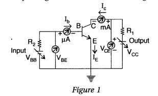
(i) Input characteristics. The variation of the base current
IB with the base emitter voltage VBE is called the input
characteristic keeping VCE fixed. A curve is plotted between the base
current IB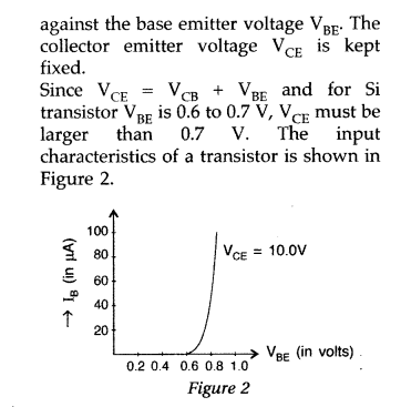
(ii) Output characteristics. The variation of the collector
current IC with the collector emitter voltage VCE, keeping
the base current IB constant is called output characteristics.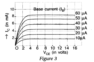
The plot of IC versus VCE for different
fixed values of IB gives one output characteristic. The different
output characteristics for different values of IB is shown in Figure
3.
Question 75.
(i) Explain with the help of a diagram the formation of
depletion region and barrier potential in a pn junction.
(ii) Draw the
circuit diagram of a half wave rectifier and explain its working. (All India
2016)
Answer:
(a) (i) Depletion layer. The layer containing unneutralized
acceptor and donor ion across a p-n junction is called depletion layer. It is
called depletion layer because it is depleted of mobile charge carriers.
(ii)
Barrier potential. The electric field between the acceptor and donor ions is
called the barrier. The difference of potential from one side of the barrier to
the other side is called barrier potential.
(i) The increase of doping
concentration will reduce width of depletion layer in semi conductor.
(ii)
depletion layer widens under reverse bias and vice versa.
(b) Rectifier. A rectifier is a circuit which converts an alternating current
into direct current.
p-n diode as a half wave rectifier. A half wave
rectifier consists of a single diode as shown in the circuit diagram. The
secondary of the transformer gives the desired a.c. voltage across A and B.
In the positive half cycle of a.c., the voltage at A is positive, the diode is
forward biased and it conducts current.
In the negative half cycle of a.c., the voltage at A is
negative, the diode is reversed biased and it does not conduct current.
Thus,
we get output across RL during positive half cycles only. The output
is unidirectional but varying.
Question 76.
For a CE-transistor amplifier, the audio signal voltage
across the collector resistance of 2kΩ is 2 V. Suppose the current amplification
factor of the transistor is 100, find the input signal voltage and base current,
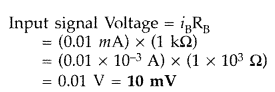
if the base resistance is 1 kΩ. (All India 2016)
Answer: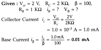
Question 77.
Give reasons for the following :
(i) High reverse voltage
do not appear across a LED.
(ii) Sunlight is not always required for the
working of a solar cell.
(ill) The electric field, of the junction of a Zener
diode, is very high even for a small reverse bias voltage of about 5V. (Comptt.
Delhi 2016)
Answer:
(i) It is because reverse breakdown voltage of LED is
very low, i.e., nearly 5V.
(ii) Solar cell can work with any light whose
photon energy is more than the band gap energy.
(iii) The heavy doping of p
and n sides of pn junction makes the depletion region very thin, hence for a
small reverse bias voltage, electric field is very high.
Question 78.
It is required to design a (two-input) logic gate, using an
appropriate number, of :
(a) NAND gates that gives a ‘low’ output only when
both the inputs are ‘low’.
(b) NOR gates that gives a ‘high’ output only when
both the inputs are ‘high’.
Draw the logic circuits for these two cases and
write the truth table, corresponding to each of the two designs. (Comptt. All
India 2017)
Answer:
(a) The ‘NAND’ gate that gives a ‘low’ output only
when both its inputs are low, is an ‘OR’ gate
The required design and the
truth table are as follow :
Truth Table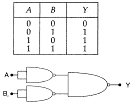
(b) The ‘NOR’ gate that gives a high output only when both the inputs are
high, is an ‘AND’ gate. The required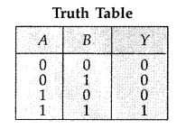
Question 79.
Write the two processes that take place in the formation of a
p-n junction. Explain with the help of a diagram, the formation of depletion
region and barrier potential in a p-n junction. (Delhi 2016)
Answer:
Diffusion and Drift are the two processes which take place in the formation of
p-n junction.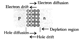
Due to the diffusion of electrons and holes across the junction, a region of (immobile) positive charge is created on the n-side and a region of (immobile) negative charge is created on the p-side, near the junction; this is called depletion region.
Barrier potential is formed due to loss of electrons from n-region and gain of electrons by p-region. Its polarity is such that it opposes the movement of charge carriers across the junction.
Question 80.
For a CE-transistor amplifier, the audio signal voltage
across the collector resistance of 2 kΩ is 2V. Given the current amplification
factor of the transistor is 100, find the input signal voltage and base current,
if the base resistance is 1 kΩ (Delhi 2017)
Answer:
Question 81.
A zener diode is fabricated by heavily doping both p- and
n-sides of the junction. Explain, why? Briefly explain the use of zener diode as
a dc voltage regulator with the help of a circuit diagram. ‘ (Delhi 2017)
Answer:
Zener Diode : By heavily doping both p and n sides of the junction,
depletion region formed is very thin, i.e. < 10-6 m. Hence,
electric field, across the junction is very high (~5 × 10⁶ V/m) even
for a small reverse bias voltage. This can lead to a ‘breakdown’ during reverse
biasing.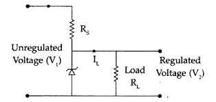
If the input voltage increases/decreases, current through
resistor RS, and Zener diode, also increases/decreases. This
increases/decreases the voltage drop across Rs without any change in voltage
across the Zener diode.
This is because, in the breakdown region, Zener voltage remains constant even though the current through the Zener diode changes.
Question 82.
Explain briefly with the help of necessary diagrams, the
forward and the reverse biasing of a p-n junction diode. Also draw their
characteristic curves in the two cases. (Delhi 2017)
Answer: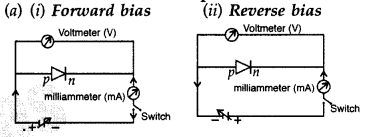
The battery is connected to the silicon diode through a
potentiometer (or rheostat), so that the applied voltage can be changed for
different values of voltages, the corresponding values of current are
noted.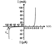
Using the circuit arrangements shown in fig. (i) and fig (ii), we study the
variation of current with applied voltage to obtain the V-I characteristics.
From the V-I characteristics of a junction diode, it is clear that it allows the
current to pass only when it is forward biased. So when an alternatively voltage
is applied across the diode, current flows only during that part of the cycle
when it is forward biased.
Question 83.
(a) In the given diagram, is the junction diode forward
biased or reverse biased?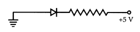
(b) Draw the circuit diagram of a full wave rectifier and
state how it work. (All India 2017)
Answer:
(a) The junction diode is
reverse biased in the given circuit diagram.
Working : The diode Dj is forward- biased during one half
cycle and current flows through the resistor, but diode D2 is
reverse-biased and no current flows through it. During the other half cycles,
current through the resistor flows in the same direction.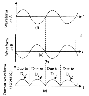
Question 84.
(a) Write the functions of the three segments of a
transistor.
(b) The figure shows the input waveforms A and B for ‘AND’ gate.
Draw the output waveform and write the truth table for this logic gate. (All
India 2017)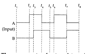
Answer:
(a) All the three segments of a transistor have
different thickness and their doping levels are also different. A brief
description of the three segments of a transistor is given below :
- Emitter: This is the segment on one side of the transistor. It is of moderate size and heavily doped. It supplies a large number of majority carriers for the current flow through the transistor.
- Base : This is the central segment. It is very thin and lightly doped.
- Collector : This segment collects a major portion of the majority carriers
supplied by the emitter. The collector side is moderately doped and larger in
size as compared to the emitter.
Question 85.
(a) In the given diagram, which bulb out of B1 and
B2 will glow and why ?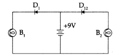
(b) Draw the circuit diagram of a full wave rectifier and
state how it works.
(c) Explain briefly the three processes due to which
generation of emf takes place in a solar cell. (All India 2017)
Answer:
(a) Bulb B1 will glow, because Diode D1 is forward
biased.
(b) Diagram of Solar Cell :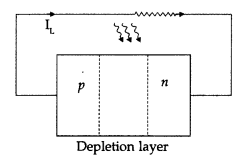
(c) Three processes in a solar cell for generation of
emf:
Generation : Incident light generates electron-hole pairs.
Separation
: Electric field of the depletion layer separates the electrons and holes.
Collection : Electrons and holes are collected at the n and p side contacts.
Question 86.
(a) Draw the circuit diagram for studying the
characteristics of a transistor in common emitter configuration. Explain briefly
and show how input and output characteristics are drawn.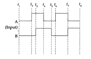
(b) The figure shows input waveforms A and B to a logic gate.
Draw the output waveform for an OR gate. Write the truth table for this logic
gate and draw its logic symbol. (All India 2017)
Answer:
(a) The base is
made very thin so as to control current flowing between emitter and collector.
The base is lightly doped to make a thin depletion layer between emitter and
collector.
(b) Common emitter (CE) transistor characteristics. The transistor is most
widely used in the CE configuration. When a transistor is used in CE
configuration, the input is between the base and emitter and the output is
between the collector and emitter.
The input and the output characteristics
of an n-p-n transistor in CE configuration can be studied by using the circuit
as shown in Figure 1.
(i) Input characteristics. The variation of the base current
IB with the base emitter voltage VBE is called the input
characteristic keeping VCE fixed. A curve is plotted between the base
current IB
(ii) Output characteristics. The variation of the collector
current IC with the collector emitter voltage VCE, keeping
the base current IB constant is called output characteristics.
The plot of IC versus VCE for different
fixed values of IB gives one output characteristic. The different
output characteristics for different values of IB is shown in Figure
3.
Question 87.
(a) Draw the circuit diagram of an n-p-n transistor
amplifier in common emitter configuration.
(b) Derive an expression for
voltage gain of the amplifier and hence show that the output voltage is in
opposite phase with the input voltage. (All India 2017)
Answer:
During the positive half cycle of input signal, the forward
bias of emitter-base junction increases.
Due to increased forward bias,
emitter current (IE) increases and hence according to equation (i)
collector current (IC) also increases. Therefore, the voltage drop
across RL (i.e. ICRL) increases. According to
equation (ii), the collector voltage or output voltage (V0)
decreases. Thus collector is connected to the positive terminal of the battery
(VCC)
so decrease in V0 means that the collector
voltage becomes 1 cm positive. In other words, amplified negative signal is
obtained across the output.
Similarly, during negative hay cycle, an
amplified positive signal is obtained across the output.
Question 88.
(a) In the given following diagram ‘S’ is a semiconductor.
Would you increase or decrease the value of R to keep the reading of the ammeter
A constant when S is heated? Give reason for your answer.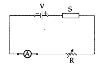
(b) The figure shows input waveforms A and B to a logic gate.
Draw the output waveform for an OR gate. Write the truth table for this logic
gate and draw its logic symbol. (All India 2017)
Answer:
(a) The value of
‘R’ would be increased since the resistance of ‘S’, a semi conductor decreases
on heating.
(b) Photo diodes. Photo diode is a special type of photo-detector. Simplest
photo-diode is a reverse biased as shown in Figure (i).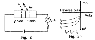
When a p-n diode is illuminated with light photons having
energy /xv > and intensities Iv I2, I3 etc. the electron and hole pairs
generating in the depletion layer will be separated by the junction field and
made to flow across the junction.
Graph showing variation in reverse bias
currents for different intensities are shown in Figure (ii).
Question 89.
Explain the two processes involved in the formulation of a
p-n junction diode. Hence define the term ‘barrier potential’. (Comptt. Delhi
2017)
Answer:
(a) Two important processes that occur during the formation
of a p-n junction are
(i) diffusion and
(ii) drift.
(i) Diffusion: In
n-type semiconductor, the concentration of electrons is much greater as compared
to concentration of holes; while in p-type semiconductor, the concentration of
holes is much greater than the concentration of electrons. When a p-n junction
is formed, then due to concentration gradient, the holes diffuse from p side to
n side (p ➝ n) and electrons diffuse from n side to p-side (n ➝ p). This motion
of charge carriers gives rise to diffusion current across the junction.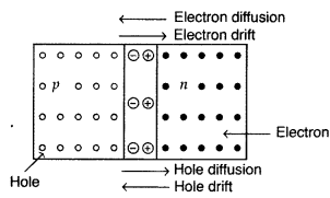
(ii) Drift: The drift of charge carriers occurs due to electric field. Due to
built in potential barrier an electric field directed from n-region to p-region
is developed across the junction. This field causes motion of electrons on
p-side of the junction to n-side and motion of holes on n-side of junction to
p-side. Thus a drift current starts. This current is opposite to the direction
of diffusion current.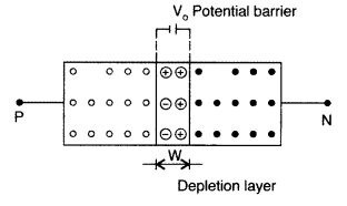
Question 90.
Using the wave forms of the input A and B, draw the output
waveform of the given logic circuit. Identify the logic gate obtained. Write
also the truth table. (Comptt. Delhi 2017)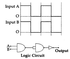
Answer: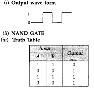
Question 91.
State the reason, why the photodiode is always operated
under reverse bias. Write the working principle of operation of a photodiode.
The semiconducting material used to fabricate a photodiode, has an energy gap of
1.2 eV. Using calculations, show whether it can detect light of wavelength of
400 nm incident on it. (Comptt. All India 2017)
Answer:
(a) Why is
photodiode fabricated?
- It is fabricated with a transparent window to allow light to fall on diode.
(b) Working of photodiode : When the
photodiode is illuminated with
photons of energy (hv > Eg) greater than the energy gap
- of the semiconductor, electron-holes pairs are generated. These get separated due to the Junction electric field (before they recombine) which produces an emf.
(c) Diagram of photodiode
(d) Reason. It is easier to observe the change in the current, with change in light intensity, if a reverse bias is applied.
Question 92.
Draw the circuit diagram of a common emitter transistor
amplifier. Write the expression for its voltage gain. Explain, how the input and
output signals differ in phase by 180°. (Comptt. All India 2017)
Answer:
During the positive half cycle of input signal, the forward
bias of emitter-base junction increases.
Due to increased forward bias,
emitter current (IE) increases and hence according to equation (i)
collector current (IC) also increases. Therefore, the voltage drop
across RL (i.e. ICRL) increases. According to
equation (ii), the collector voltage or output voltage (V0)
decreases. Thus collector is connected to the positive terminal of the battery
(VCC)
so decrease in V0 means that the collector
voltage becomes 1 cm positive. In other words, amplified negative signal is
obtained across the output.
Similarly, during negative hay cycle, an
amplified positive signal is obtained across the output.
From the circuit diagram, we find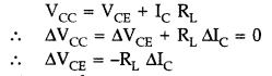
Hence, change in output is negative when the input signal is
positive.
This shows that input and output signals differ in phase by
180°.
Question 93.
Draw the circuit diagram of a full wave rectifier. Explain
its working principle. Draw the input and output waveforms. (Comptt. All India
2017)
Answer:
Working of a full wave rectifier :
1. A full wave
rectifier uses two diodes and gives the rectified output voltage corresponding
to both the positive and negative half-cycle of alternating current.
2. The
p-side of the two diodes are connected to the ends of the secondary of the
transformer and, the n-sides of the diodes are connected together.
3. Output
is taken from between the common- point of the two diodes and secondary of the
transformer. Hence, the secondary of the transformer is provided with center
tapping and is also called the centre-tap transformer.
4. Let, the input
voltage to A with respect to the centre be positive and, at the same instant,
voltage at B being out-of-phase will be negative. Therefore, diode D1
is forward biased and starts conducting whereas, D2 being reverse
biased does not conduct.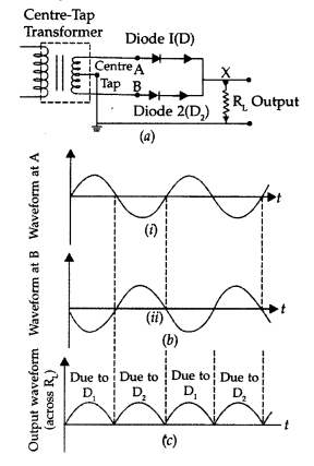
5. Thus, we get an output current and an output voltage
across the load resistance RL in the first positive half-cycle.
6. During the
course of the negative half-cycle, that is, when voltage at A becomes negative
and voltage at B becomes positive, we will have D1 as reverse biased
and D2 forward biased.
7. In the negative part of the cycle, only
diode D2 will conduct giving an output current and output voltage
across RL.
8. For both positive and negative half cycle we will
get the output voltage. This rectified output voltage has the shape of half
sinusoids.
Question 94.
Draw the V-I characteristic of an LED. State two advantages
of LED lamps over conventional incandescent lamps. Write the factor which
controls
(a) wavelength of light emitted,
(b) intensity of light emitted
by an LED. (Comptt. All India 2017)
Answer: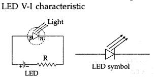
Light Emitting Diode (LED) : A light emitting diode is simply a forward
biased p-n junction which emits spontaneous light radiation. When forward bias
is applied, the electron and holes at the junction recombine and energy released
is emitted in the form of light. V-I characteristics of LED are similar to that
of Si junction diode but the threshold voltages are much higher and slightly
different for each colour. No conduction or light emission occurs for reverse
bias which, if it exceeds 5V, may damage the LED.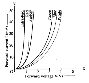
Advantages of LED over conventional lamps :
(i) Low
operational voltage.
(ii) Less power consumption.
(iii) Long life.
(iv)
Ruggedness
Controlling factors :
(a) Energy band gap controls the
wavelength of light emitted.
(b) Forward current controls the intensity of
emitted light.
Question 95.
Two semiconductor materials X and Y showed in the figure are
made by doping germanium crystal with indium and arsenic respectively. The two
are joined end to end and connected to a battery as shown,
(i) Will the
junction be forward or reverse biased?
(ii) Sketch a V-l graph for this
arrangement.
Answer:
Material X is p-type and material Y is n-type.
(i) The junction is
reverse biased.
(ii) For the V-l graph
The characteristics are as
shown.
Question 96.
Draw the output waveform across the resistor (figure).
(NCERT)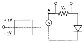
Answer:
It is a half-wave rectifier, therefore only the positive cycle will
be rectified. Thus the output waveform is as shown.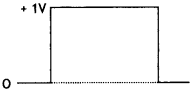
Question 97.
(i) Name the type of a diode whose characteristics are shown in
figure
(a) and figure (b).
(ii) What does point P in figure (a)
represent?
(iii) What do the points P and Q in figure (b) represent? (NCERT
Exemplar)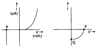
Answer:
(i) Zener junction diode and solar cell.
(ii) Zener breakdown
voltage
(iii) P-open circuit voltage.
Q-short circuit current
Question 98.
A Zener of power rating 1 W is to be used as a voltage
regulator. If Zener has a breakdown of 5 V and it has to regulate voltage which
fluctuated between 3 V and 7 V, what should be the value of R, for safe
operation (figure)? (NCERT Exemplar)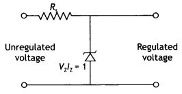
Answer:
Given P = 1 W, Vz = 5V, Vs = 7 V, Rs = ?
We know that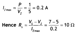
Question 99.
Two material bars A and B of the equal area of the cross-section
are connected in series to a dc supply. A is made of usual resistance wire and B
of an n-type semiconductor.
(i) In which bar is the drift speed of free
electrons greater?
(ii) If the same constant current continues to flow for a
long time, how will the voltage drop across A and B be affected? Justify each
answer. (CBSE Sample Paper 2018-19)
Answer:
(i) Drift speed in B (n-type
semiconductor) is higher.
Reason: Since the two bars A and B are connected in
series, the current through each is the same.
Now l = neAvd
Or
vd = \(\frac{1}{n e A}\) ⇒ vd ∝ \(\frac{1}{n}\) (As
l and A are same).
As n is much lower in semiconductors, drift velocity will be more.
Question 100.
Explain how the width of the depletion layer in a p-n
junction diode changes when the junction is (i) forward biased and (ii) reverse
biased. (CBSE Delhi 2018C)
Answer:
The width of the depletion region in a
p-n junction diode decreases when it is forward biased because the majority of
charge carriers flow towards the junction. While it increases when the junction
diode is reverse biased because the majority of charge carriers move away from
the junction.
Long Answer Type
Question 1.
Define the terms ‘potential barrier’ and ‘depletion region’
for a p – n junction diode. State how the thickness of the depletion region will
change when the p-n junction diode is (i) forward biased and (ii) reverse
biased.
Answer:
Potential barrier: The potential barrier is the fictitious
battery, which seems to be connected across the p-n junction with its positive
terminal in the n-region and the negative terminal in the p-region.
Depletion region: The region around the junction, which is devoid of any mobile charge carriers, is called the depletion layer or region.
- When the p-n junction is forward biased, there is a decrease in the depletion region.
- When the p-n junction is reverse biased, there is an increase in the depletion region.
Question 2.
(i) Draw a circuit diagram to study the input and output
characteristics of an n-p-n transistor in its common emitter configuration. Draw
the typical input and output characteristics.
(ii) Explain, with the help of
a circuit diagram, the working of n-p-n transistor as a common emitter
amplifier. (Delhi 2017)
Answer.
(i) (a) Common emitter configuration of
n-p-n transistor
(ii) Transistor as an amplifier (C.E. configuration) : The
circuit diagram of a common emitter amplifier using n-p-n transistor is given
below :
The input (base-emitter) circuit is forward biased and the
output circuit (collector- emitter) is reverse biased.
When no a.c. signal is
applied, the potential difference VCC between the collector and
emitter is given by![]()
When an a.c. signal is fed to the input circuit, the forward
bias increases during the positive half cycle of the input. This results in
increase in IC and decreases in VCC. Thus during positive
half cycle of the input, the collector becomes less positive.
During the negative half cycle of the input, the forward bias is decreased
resulting in decrease in IE and hence IC. Thus
VCC would increase making the collector more positive. Hence in a
common-emitter amplifier, the output voltage is 180° out of phase with the input
voltage.![]()
Question 3.
How is a zener diode fabricated so as to make it a special
purpose diode? Draw I-V characteristics of zener diode and explain the
significance of breakdown voltage.
Explain briefly, with the help of a
circuit diagram, how a p-n junction diode works as a half wave rectifier.
Answer:
Zener diode is fabricated by heavily doping both p and n-sides. Due
to this, depletion region formed is very thin (< 10-6 n and the
electric field of the junction is extremely high (~5 × 10⁶ V / m)
even for a small reverse bias voltage of 5 volts. It is seen that when the
applied reverse bias voltage (V) reaches the breakdown voltage (Vz) of the Zener
diode, there is a large change in the current. After the breakdown voltage Vz, a
large change in the current can be produced by almost insignificant change in
the reverse bias voltage. In other words, Zener voltage remains constant even
though current through the Zener diode varies over a wide range.
This property of the Zener diode is used for regulating voltages so that they
are constant. Semiconductor diode as a half wave Rectifier : The junction diode
D, supplies rectified current to the band during one half of the alternating
input voltage and is always in the same direction. During the first half cycles
of the alternating input voltage, junction diodes D1 will conduct
each permitting current to flow during one half cycle whenever its p-terminal is
positive with respect to the n-terminal.
The resulting output current is a series of unidirectional
pulses with alternate gaps.
Question 4.
(a) Explain the formation of depletion layer . and potential
barrier in a p-n junction.
(b) In the figure given below the input waveform is converted
into the output waveform by a device ‘X’. Name the device and draw its circuit
diagram.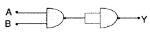
(c) Identify the logic gate represented by the circuit as
shown and write its truth table. (Delhi 2017)
Answer:
(a)
As soon as a
p-n junction is formed, the majority charge carriers begin to diffuse from the
regions of higher concentration to the regions of lower concentrations. Thus the
electrons from the n-region diffuse into the p-region and where they combine
with the holes and get neutralised. Similarly, the holes from the p-region
diffuse into the n-region where they combine with the electrons and get
neutralised. This process is called electron-hole recombination.
The p-region near the junction is left with immobile -ve ions
and n-region near the junction is left with +ve ions as shown in the figure. The
small region in the vicinity of the junction which is depleted of free charge
carriers and has only immobile ions is called the depletion layer. In the
depletion region, a potential difference VB is created, called potential barrier
as it creates an electric field which opposes the further diffusion of electrons
and holes.
(i) In forward biased, the width of depletion region is
decreased.
(ii) In reverse biased, the width of depletion region is
increased.
(b) Device ‘X’ given here represents the full wave rectifier.
Working of
full wave rectifier : AC input to be rectified is applied to the primary (P) of
a step up transformer. Two ends of the secondary of the transformer are
connected to P end of two junction diodes. It is centre-trapped at M which is
connected to an end through the load resistance RL. Two
crystals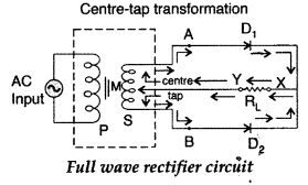
are formed biased and reverse biased alternately. During half
cycle of A.C. input, current flows through one crystal diode and during the next
half cycle the current flows through the other crystal diode. However across the
load RL, current always flows in the same direction. Thus a
continuous pulsating D.C. output voltage is obtained across the load resistance
RL. This rectified signal is made smooth with the help of the fitter
circuit.
(c) Logic gate is AND gate. Truth table of AND gate is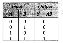
Question 5.
(a) With the help of the circuit diagram explain the working
principle of a transistor amplifier as an oscillator.
(b) Distinguish between
a conductor, a semiconductor and an insulator on the basis of energy band
diagrams. (Delhi 2017)
Answer:
(a)
Principle of transistor oscillator :
“Sustained a.c. signals can he obtained from an amplifier circuit without any
external input signal by giving a positive feedback to the input circuit through
inductive coupling or RC/LC network.”
Oscillator action : In an ideal n-p-n biased transistor, when input base
emitters junction and output base collector junction are forward and reverse
biased respectively, a high collector current IC flows through the
circuit. If in circuit switch S is on, this current IC will start
flowing in the emitter circuit through the inductive coupling between coils
T1 and T2, which provides the +ve feedback output to input
and hence make IE maximum. In the absence of +ve feedback the IE thus
decreases making the circuit back to its original state. This process continues
and ocillations are produced.
(b) Conductors :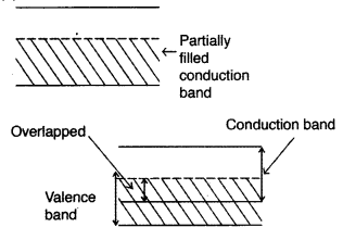
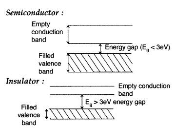
Question 6.
(a) Draw the circuit diagrams of a p-n junction diode in
(i) forward bias,
(ii) reverse bias. How are these circuits used to study the
V – I characteristics of a silicon diode? Draw the typical V – I
characteristics.
(b) What is a light emitting diode (LED)?
Mention two
important advantages of LEDs over conventional lamps. (All India 2017)
Answer:
The battery is connected to the silicon diode through a
potentiometer (or rheostat), so that the applied voltage can be changed for
different values of voltages, the corresponding values of current are
noted.
Using the circuit arrangements shown in fig. (i) and fig (ii), we study the
variation of current with applied voltage to obtain the V-I characteristics.
From the V-I characteristics of a junction diode, it is clear that it allows the
current to pass only when it is forward biased. So when an alternatively voltage
is applied across the diode, current flows only during that part of the cycle
when it is forward biased.
(b) Light emitting diode (LED) is a heavily doped p-n junction which under
forward bias emits spontaneous radiations.
Two important advantages of
LEDs:
(i) Low operational voltage and less power.
(ii) Fast on-off
switching capacity.
Question 7.
(a) Draw the circuit arrangement for studying the input and
output characteristics of an n- p-n transistor in CE configuration. With the
help of these characteristics define
(i) input resistance,
(ii) current
amplification factor.
(b) Describe briefly with the help of a circuit diagram
how an n-p-n transistor is used to produce self-sustained oscillations. (All
India 2017)
Answer:
(a) Circuit for studying the common emitter
characteristics of an n-p-n transistor :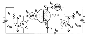
(i) Input resistance : The input resistance r, of the
transistor in CE configuration is defined as the ratio of the small change in
base-emitter voltage to the corresponding small change in the base current, when
the collector-emitter voltage is kept fixed.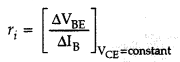
(ii) Current amplification factor (β) : It is defined as the
ratio of the change in collector current to the small change in base current at
constant collector emitter voltage (VCE) when the transistor is in
the active state.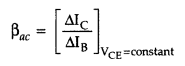
(b)
Principle of transistor oscillator : “Sustained a.c.
signals can he obtained from an amplifier circuit without any external input
signal by giving a positive feedback to the input circuit through inductive
coupling or RC/LC network.”
Oscillator action : In an ideal n-p-n biased transistor, when input base
emitters junction and output base collector junction are forward and reverse
biased respectively, a high collector current IC flows through the
circuit. If in circuit switch S is on, this current IC will start
flowing in the emitter circuit through the inductive coupling between coils
T1 and T2, which provides the +ve feedback output to input
and hence make IE maximum. In the absence of +ve feedback the IE thus
decreases making the circuit back to its original state. This process continues
and ocillations are produced.
Question 8.
Draw a simple circuit of a CE transistor amplifier. Explain
its working. Show that the voltage gain, Av, of the amplifier is given by
\(\mathbf{A}_{\mathbf{v}}=-\frac{\boldsymbol{\beta}_{a \mathbf{c}}
\mathbf{c}_{\mathbf{L}}}{r_{i}}\), where βac is the current gain,
RL is the load resistance and ri is the input resistance
of the transistor. What is the significance of the negative sign in the
expression for the voltage gain? (Delhi 2012)
Answer:
n-p-n transistor as
a common emitter amplifier : Working: According to Kirchoff’s law, emitter
current It, base current (IB) and collector current
(IC) are related as It = IB + IC
…(i)
When current (IC ) flows through the load resistance
(RL),
Output or collector voltage (V0)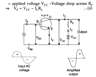
During the positive half cycle of input signal, the forward
bias of emitter-base junction increases. Due to increased forward bias, emitter
current (IE) increases and hence according to equation (i) collector
current (IC) also increases. Therefore, the voltage drop across
RL (i.e. ICRL) increases. According to equation
(ii), the collector voltage or output voltage (V0) decreases. Thus
collector is connected to the positive terminal of the battery (VCC),
so decrease in V0 means that the collector voltage becomes 1 cm
positive. In other words, amplified negative signal is obtained across the
output.
Similarly, during negative hay cycle, an amplified positive signal is
obtained across the output.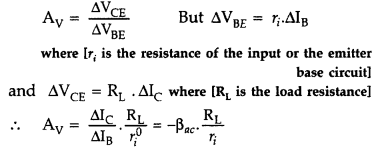
Question 9.
(a) Draw the circuit diagram of a full wave rectifier using
p-n junction diode. Explain its working and show the output, input
waveforms.
(b) Show the output waveforms (Y) for the following inputs A and B
of
(i) OR gate
(ii) NAND gate. (Delhi 2012)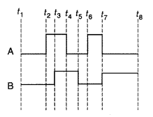
Answer:
p-n junction diode as full wave rectifier
A
full wave rectifier consists of two diodes and special type of transformer known
as centre tap transformer as shown in the circuit. The secondary of transformer
gives the desired a.c. voltage across A and B.
During the positive half cycle
of a.c. input, the diode D1 is in forward bias and conducts current
while D2 is in reverse biased and does not conduct current. So we get
an output voltage across the load resistor RL.
During the negative half cycle of a.c. input, the diode
D1 is in reverse biased and does not conduct current while diode
D2 in forward biased and conducts current. So we get an output
voltage across the load resistor RL.
NOTE: This is a more
efficient circuit for getting rectified voltage or current.
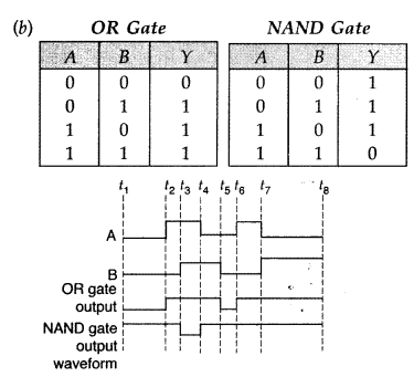
Question 110.
(a) Describe briefly, with the help of a diagram, the role
of the two important processes involved in the formation of a p-n junction:
(b) Name the device which is used as a voltage regulator. Draw the necessary
circuit diagram and explain its working. (All India 2012)
Answer:
(a) Two
important processes that occur during the formation of a p-n junction are
(i)
diffusion and
(ii) drift.
(i) Diffusion: In n-type semiconductor, the
concentration of electrons is much greater as compared to concentration of
holes; while in p-type semiconductor, the concentration of holes is much greater
than the concentration of electrons. When a p-n junction is formed, then due to
concentration gradient, the holes diffuse from p side to n side (p ➝ n) and
electrons diffuse from n side to p-side (n ➝ p). This motion of charge carriers
gives rise to diffusion current across the junction.
(ii) Drift: The drift of charge carriers occurs due to electric field. Due to
built in potential barrier an electric field directed from n-region to p-region
is developed across the junction. This field causes motion of electrons on
p-side of the junction to n-side and motion of holes on n-side of junction to
p-side. Thus a drift current starts. This current is opposite to the direction
of diffusion current.
(b) Zener diode is used as voltage regulator.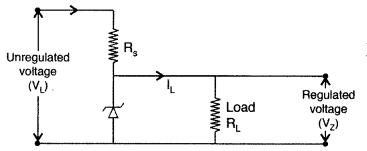
Any increase/decrease in the input voltage results in
increase/decrease of the voltage drop across Rs without any change in voltage
across the zener diode. Thus, the zener diode acts as a voltage regulator.
Question 111.
(a) Explain briefly the principle on which a
transistor-amplifier works as an oscillator. Draw the necessary circuit diagram
and explain its working.
(b) Identify the equivalent gate for the following
circuit and write its truth table. (All India 2012)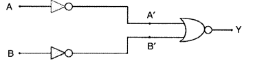
Answer:
(a)
Principle of transistor oscillator :
“Sustained a.c. signals can he obtained from an amplifier circuit without any
external input signal by giving a positive feedback to the input circuit through
inductive coupling or RC/LC network.”
Oscillator action : In an ideal n-p-n biased transistor, when input base
emitters junction and output base collector junction are forward and reverse
biased respectively, a high collector current IC flows through the
circuit. If in circuit switch S is on, this current IC will start
flowing in the emitter circuit through the inductive coupling between coils
T1 and T2, which provides the +ve feedback output to input
and hence make IE maximum. In the absence of +ve feedback the IE thus
decreases making the circuit back to its original state. This process continues
and ocillations are produced.
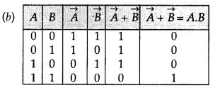
Name of gate : AND Gate
Question 112.
The set-up shown below can produce an a.c. output without
any external input signal. Identify the components ‘X’ and ‘Y’ of this set-up.
Draw the circuit diagram for this set-up. Describe briefly its working.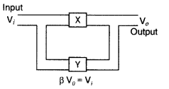
Answer:
The component X is Amplifier (Transistor
Amplifier).
The component Y is (positive) Feedback Network. Circuit diagram
and its working.
Principle of transistor oscillator : “Sustained a.c. signals can he obtained from an amplifier circuit without any external input signal by giving a positive feedback to the input circuit through inductive coupling or RC/LC network.”
Oscillator action : In an ideal n-p-n biased transistor, when input base
emitters junction and output base collector junction are forward and reverse
biased respectively, a high collector current IC flows through the
circuit. If in circuit switch S is on, this current IC will start
flowing in the emitter circuit through the inductive coupling between coils
T1 and T2, which provides the +ve feedback output to input
and hence make IE maximum. In the absence of +ve feedback the IE thus
decreases making the circuit back to its original state. This process continues
and ocillations are produced.
Question 113.
(a) Explain the formation of depletion region for p-n
junction diode. How does the width of this region change when the junction
is
(i) forward biased,
(ii) reverse biased?
(b) Draw the circuit
diagram of a full wave rectifier. Briefly explain its working. (Comptt. All
India 2012)
Answer:
(a)
As soon as a p-n junction is formed, the
majority charge carriers begin to diffuse from the regions of higher
concentration to the regions of lower concentrations. Thus the electrons from
the n-region diffuse into the p-region and where they combine with the holes and
get neutralised. Similarly, the holes from the p-region diffuse into the
n-region where they combine with the electrons and get neutralised. This process
is called electron-hole recombination.
The p-region near the junction is left with immobile -ve ions
and n-region near the junction is left with +ve ions as shown in the figure. The
small region in the vicinity of the junction which is depleted of free charge
carriers and has only immobile ions is called the depletion layer. In the
depletion region, a potential difference VB is created, called potential barrier
as it creates an electric field which opposes the further diffusion of electrons
and holes.
(i) In forward biased, the width of depletion region is
decreased.
(ii) In reverse biased, the width of depletion region is
increased.
(b) Device ‘X’ given here represents the full wave rectifier.
Working of
full wave rectifier : AC input to be rectified is applied to the primary (P) of
a step up transformer. Two ends of the secondary of the transformer are
connected to P end of two junction diodes. It is centre-trapped at M which is
connected to an end through the load resistance RL. Two
crystals
are formed biased and reverse biased alternately. During half
cycle of A.C. input, current flows through one crystal diode and during the next
half cycle the current flows through the other crystal diode. However across the
load RL, current always flows in the same direction. Thus a
continuous pulsating D.C. output voltage is obtained across the load resistance
RL. This rectified signal is made smooth with the help of the fitter
circuit.
Question 114.
(a) Why is the base region of a transistor thin and lightly
doped?
(b) Draw the circuit diagram for studying the characteristics of an
n-p-n transistor in com-mon emitter configuration.
Sketch the typical
(i)
input and
(ii) output characteristics in this configuration.
(c) Describe
briefly how the output characteristics can be used to obtain the current gain in
the transistor. (Comptt. Delhi 2012)
Answer:
(a) The base is made very
thin so as to control current flowing between emitter and collector. The base is
lightly doped to make a thin depletion layer between emitter and collector.
(b) Common emitter (CE) transistor characteristics. The transistor is most
widely used in the CE configuration. When a transistor is used in CE
configuration, the input is between the base and emitter and the output is
between the collector and emitter.
The input and the output characteristics
of an n-p-n transistor in CE configuration can be studied by using the circuit
as shown in Figure 1.
(i) Input characteristics. The variation of the base current
IB with the base emitter voltage VBE is called the input
characteristic keeping VCE fixed. A curve is plotted between the base
current IB
(ii) Output characteristics. The variation of the collector
current IC with the collector emitter voltage VCE, keeping
the base current IB constant is called output characteristics.
The plot of IC versus VCE for different
fixed values of IB gives one output characteristic. The different
output characteristics for different values of IB is shown in Figure
3.
Question 115.
(a) How is a depletion region formed in p-n junction?
(b)
With the help of a labelled circuit diagram, explain how a junction diode is
used as a full wave rectifier.
Draw its input, output wave-forms.
(c) How
do you obtain steady d.c. output from the pulsating voltage? (Comptt. Delhi
2012)
Answer:
(a) p-n junction. When a small piece of III group metal like
In (Indium) is placed over n – Ge or n – Si and melted, the lower portion of
molten indium forms alloy with
n-semiconductor and converts its top layer
into p-layer to form p-n junction.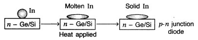
Formation of depletion region in a p-n junction. In a p-n
junction diode, due to higher concentration of holes on p-side and electrons on
n-side, the diffusion of holes towards n-side and electrons towards p-side takes
place.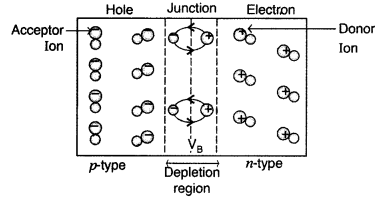
Hence, a region of unneutralized negative ions on p-side and
positive ions on n-side is formed near the junction which is depleted of mobile
charges. This region is called depletion region.
(b) p-n junction diode as full wave rectifier. A full wave rectifier consists
of two diodes and special type of transformer known as centre tap transformer as
shown in the circuit. The secondary of transformer gives the desired a.c.
voltage across A and B.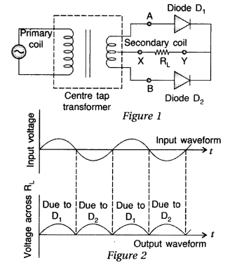
During the positive half cycle of a.c. input, the diode
D1 is in forward bias and conducts current while D2 is in
reverse biased and does not conduct current. So we get an output voltage across
the load resistor RL. During the negative half cycle of a.c. input,
the diode D1, is in reverse biased and does not conduct current while
diode D2 is in forward biased and conducts current. So we get an
output voltage across the load resistor RL.
(c) Using capacitive filter circuits connected in parallel to get a pure d.c. output.
Question 116.
(a) Define the terms ‘depletion layer’ and ‘barrier
potential’ for a p-n junction. How does
(i) an increase in the doping
concentration and
(ii) biasing across the junction, affect the width of the
depletion layer?
(b) Draw the circuit diagram of a p-n diode used as a
half-wave rectifier. Explain its working. (Comptt. All India 2012)
Answer:
(a) (i) Depletion layer. The layer containing unneutralized acceptor
and donor ion across a p-n junction is called depletion layer. It is called
depletion layer because it is depleted of mobile charge carriers.
(ii)
Barrier potential. The electric field between the acceptor and donor ions is
called the barrier. The difference of potential from one side of the barrier to
the other side is called barrier potential.
(i) The increase of doping
concentration will reduce width of depletion layer in semi conductor.
(ii)
depletion layer widens under reverse bias and vice versa.
(b) Rectifier. A rectifier is a circuit which converts an alternating current
into direct current.
p-n diode as a half wave rectifier. A half wave
rectifier consists of a single diode as shown in the circuit diagram. The
secondary of the transformer gives the desired a.c. voltage across A and B.
In the positive half cycle of a.c., the voltage at A is positive, the diode is
forward biased and it conducts current.
In the negative half cycle of a.c., the voltage at A is
negative, the diode is reversed biased and it does not conduct current.
Thus,
we get output across RL during positive half cycles only. The output
is unidirectional but varying.
Question 117.
(a) Briefly explain with the help of a circuit diagram how
input and output characteristics of n-p-n transistor in CE configuration are
obtained.
(b) Draw the transfer characteristics of a transistor in CE
configuration. Explain how it is used in the working of the transistor as an
amplifier and a switch. (Comptt. All India 2012)
Answer:
(a) Common
emitter (CE) transistor characteristics. The transistor is most widely used in
the CE configuration. When a transistor is used in CE configuration, the input
is between the base and emitter and the output is between the collector and
emitter.
The input and the output characteristics of an n-p-n transistor in
CE configuration can be studied by using the circuit as shown in Figure
1.
(i) Input characteristics. The variation of the base current
IB with the base emitter voltage VBE is called the input
characteristic keeping VCE fixed. A curve is plotted between the base
current IB
(ii) Output characteristics. The variation of the collector
current IC with the collector emitter voltage VCE, keeping
the base current IB constant is called output characteristics.
The plot of IC versus VCE for different
fixed values of IB gives one output characteristic. The different
output characteristics for different values of IB is shown in Figure
3.
(b) Transistor as a switch. The circuit diagram of transistor
as a switch is shown in Figure 1.
Transfer characteristics. The graph between
V0 and V1 is called the. transfer characteristics of the
base-biased transistor, shown in Figure 2.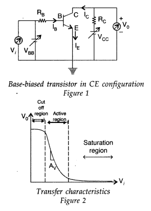
When the transistor is used in the cut off or saturation
state, it acts as a switch.
As long as V; is loio and unable to forward bias
the transistor, then V0 is high. If V; is high enough to drive the transistor
into saturation, then V0 is low. When the transistor is not conducting, it is
said to be sivitched off and when it is driven into saturation, it is said to be
switched on. This shows that a low input switches the transistor off and a high
input switches it on.
Question 118.
(a) State briefly the processes involved in the formation of
p-n junction explaining clearly how the depletion region is formed.
(b) Using
the necessary circuit diagrams, show how the V-I characteristics of a p-n
junction are obtained in
(i) Forward biasing
(ii) Reverse biasing How are
these characteristics made use of in rectification? (Delhi 2012)
Answer:
(a) p-n junction and depletion regions. Two processes involved during the
formation of p-n junction are diffusion and drift. Due to the concentration
gradient, across p and n sides of the junction, holes diffuse from p ➝ n, and
electrons from n ➝ p. This movement of charge carriers leaves behind ionised
acceptors on the p-side and donors on the n-side of the junction. This space
charge region on either side of the junction, together, is known as depletion
region.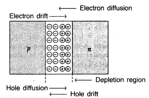
(b)
The battery is connected to the silicon diode through a
potentiometer (or rheostat), so that the applied voltage can be changed for
different values of voltages, the corresponding values of current are
noted.
Using the circuit arrangements shown in fig. (i) and fig (ii), we study the
variation of current with applied voltage to obtain the V-I characteristics.
From the V-I characteristics of a junction diode, it is clear that it allows the
current to pass only when it is forward biased. So when an alternatively voltage
is applied across the diode, current flows only during that part of the cycle
when it is forward biased.
“These characteristic make use of p-n junction diode as a rectifier. In the positive half cycle of ac, the voltage is positive and the diode is forward biassed and it conducts current. While in the negative half cycle of ac, the voltage is negative, the diode is reverse biassed and it does not conduct current. Thus we get rectified output during positive half cycles only. The output is unidirectional, but varying.”
Question 119.
(a) Differentiate between three segments of a transistor on
the basis of their size and level of doping.
(b) How is a transistor biased
to be in active state?
(c) With the help of necessary circuit diagram,
describe briefly how tt-p-n transistor in CE configuration amplifies a small
sinusoidal input voltage. Write the expression for the ac current gain. (Delhi
2012)
Answer:
(a) All the three segments of a transistor have different
thickness and their doping levels are also different. A brief description of the
three segments of a transistor is given below :
- Emitter: This is the segment on one side of the transistor. It is of moderate size and heavily doped. It supplies a large number of majority carriers for the current flow through the transistor.
- Base : This is the central segment. It is very thin and lightly doped.
- Collector : This segment collects a major portion of the majority carriers supplied by the emitter. The collector side is moderately doped and larger in size as compared to the emitter.
(b) When the transistor works as an amplifier, with its emitter-base junction forward biased; and the base-collector junction reverse biased, is said to be in Active state.
(c) n-p-n transistor as amplifier.
n-p-n transistor as a common emitter
amplifier : Working: According to Kirchoff’s law, emitter current It,
base current (IB) and collector current (IC) are related
as It = IB + IC …(i)
When current (IC
) flows through the load resistance (RL),
Output or
collector voltage (V0)
During the positive half cycle of input signal, the forward
bias of emitter-base junction increases. Due to increased forward bias, emitter
current (IE) increases and hence according to equation (i) collector
current (IC) also increases. Therefore, the voltage drop across
RL (i.e. ICRL) increases. According to equation
(ii), the collector voltage or output voltage (V0) decreases. Thus
collector is connected to the positive terminal of the battery (VCC),
so decrease in V0 means that the collector voltage becomes 1 cm
positive. In other words, amplified negative signal is obtained across the
output.
Similarly, during negative hay cycle, an amplified positive signal is
obtained across the output.
Question 120.
(a) Explain with the help of a diagram, how a depletion
layer and barrier potential are formed in a junction diode.
(b) Draw a
circuit diagram of a full wave rectifier. Explain its working and draw input and
output waveforms. (Comptt. Delhi 2012)
Answer:
(a)
As soon as a p-n
junction is formed, the majority charge carriers begin to diffuse from the
regions of higher concentration to the regions of lower concentrations. Thus the
electrons from the n-region diffuse into the p-region and where they combine
with the holes and get neutralised. Similarly, the holes from the p-region
diffuse into the n-region where they combine with the electrons and get
neutralised. This process is called electron-hole recombination.
The p-region near the junction is left with immobile -ve ions
and n-region near the junction is left with +ve ions as shown in the figure. The
small region in the vicinity of the junction which is depleted of free charge
carriers and has only immobile ions is called the depletion layer. In the
depletion region, a potential difference VB is created, called potential barrier
as it creates an electric field which opposes the further diffusion of electrons
and holes.
(i) In forward biased, the width of depletion region is
decreased.
(ii) In reverse biased, the width of depletion region is
increased.
(b)
p-n junction diode as full wave rectifier
A full wave rectifier
consists of two diodes and special type of transformer known as centre tap
transformer as shown in the circuit. The secondary of transformer gives the
desired a.c. voltage across A and B.
During the positive half cycle of a.c.
input, the diode D1 is in forward bias and conducts current while
D2 is in reverse biased and does not conduct current. So we get an
output voltage across the load resistor RL.
During the negative half cycle of a.c. input, the diode
D1 is in reverse biased and does not conduct current while diode
D2 in forward biased and conducts current. So we get an output
voltage across the load resistor RL.
NOTE: This is a more
efficient circuit for getting rectified voltage or current.
Question 121.
(a) Explain briefly, with the help of a circuit diagram how
an n-p-n transistor in C.E. configuration is used to study input and output
characteristics.
(b) Describe briefly the underlying principle of a
transistor amplifier working as an oscillator. Hence, use the necessary circuit
diagram to explain how self sustained oscillations are achieved in the
oscillator. (Comptt. Delhi 2012)
Answer:
(a)
(i) (a) Common emitter
configuration of n-p-n transistor
(b)
Principle of transistor oscillator : “Sustained a.c.
signals can he obtained from an amplifier circuit without any external input
signal by giving a positive feedback to the input circuit through inductive
coupling or RC/LC network.”
Oscillator action : In an ideal n-p-n biased transistor, when input base
emitters junction and output base collector junction are forward and reverse
biased respectively, a high collector current IC flows through the
circuit. If in circuit switch S is on, this current IC will start
flowing in the emitter circuit through the inductive coupling between coils
T1 and T2, which provides the +ve feedback output to input
and hence make IE maximum. In the absence of +ve feedback the IE thus
decreases making the circuit back to its original state. This process continues
and ocillations are produced.
Question 122.
(a) Draw the circuit arrangement for studying . the V- I
characteristics of a p-n junction diode in
(i) forward and
(ii) reverse
bias. Briefly explain how the typical V-I characteristics of a diode are
obtained and draw these characteristics.
(b) With the help of necessary
circuit diagram explain the working of a photo diode used for detecting optical
signals. (Comptt. All India 2012)
Answer:
The battery is connected to the silicon diode through a
potentiometer (or rheostat), so that the applied voltage can be changed for
different values of voltages, the corresponding values of current are
noted.
Using the circuit arrangements shown in fig. (i) and fig (ii), we study the
variation of current with applied voltage to obtain the V-I characteristics.
From the V-I characteristics of a junction diode, it is clear that it allows the
current to pass only when it is forward biased. So when an alternatively voltage
is applied across the diode, current flows only during that part of the cycle
when it is forward biased.
(b) Photo diodes. Photo diode is a special type of photo-detector. Simplest
photo-diode is a reverse biased as shown in Figure (i).
When a p-n diode is illuminated with light photons having
energy /xv > and intensities Iv I2, I3 etc. the electron and hole pairs
generating in the depletion layer will be separated by the junction field and
made to flow across the junction.
Graph showing variation in reverse bias
currents for different intensities are shown in Figure (ii).
Question 123.
(a) Draw the circuit diagram of an n-p-n transistor with
emitter-base junction forward biased and collector-base junction reverse biased.
Describe briefly how the motion of charge carriers in the transistor constitutes
the emitter current (IE), the base current (IB) and the
collector current (IC). Hence deduce the relation IE =
IB + IC.
(b) Explain with the help of circuit diagram
how a transistor works as an amplifier. (Comptt. All India 2012)
Answer:
(a) In a p-n-p transitor, the heavily doped emitter which is p-type has a
majority charge carrier of holes. These holes when move towards 21-type base get
neutralized by e– in base. The majority carriers enter the base
region in large numbers. As the base is thin and lightly doped, the majority
carriers (holes) swamp the small number of electrons there and as the collector
is reverse biased, these holes can easily cross the junction and enter the
collector.
Also read the following :
The function of emitter is to
emit the majority carriers and collector is to collect the majority carriers.
Base provides the proper interaction between the emitter and the
collector.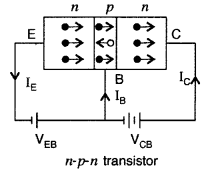
Action of n-p-n transistor. The emitter-base junction of a
transistor is forward biased while collector base junction is reverse biased as
shown in adjoining Figure.
In case of n-p-n transistor, the negative terminal of VEB repels the electrons of the emitter towards the base and constitute emitter current IE. About 5% of the electrons combine with the holes of the base to give small base current IB.
The remaining 95% of the electrons enter the collector region under the reverse bias and constitute collector current IC.
According to Kirchhoff’s law, the emitter current is the sum of collector
current and base current.
IE = IC + IB
(b)
(i) Common emitter configuration of n-p-n transistor
Question 124.
(a) Figure shows the input waveform which is converted by a
device ‘X’ into an output waveform. Name the device and explain its working
using the proper circuit Derive the expression for its voltage gain and power
gain.
(b) Draw the transfer characteristic of a base biased
transistor in CE configuration. Explain clearly which region of the curve is
used in an amplifier. (Comptt. Delhi 2015)
Answer:
(a) (i) Name of device
is common emitter amplifier.
(ii) Circuit diagram.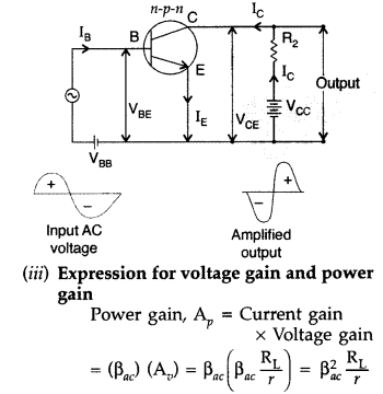
(b) Transistor as a switch. The circuit diagram of transistor as a switch is
shown in Figure 1.
Transfer characteristics. The graph between V0
and V1 is called the. transfer characteristics of the base-biased
transistor, shown in Figure 2.
When the transistor is used in the cut off or saturation
state, it acts as a switch.
As long as V; is loio and unable to forward bias
the transistor, then V0 is high. If V; is high enough to drive the
transistor into saturation, then V0 is low. When the transistor is
not conducting, it is said to be sivitched off and when it is driven into
saturation, it is said to be switched on. This shows that a low input switches
the transistor off and a high input switches it on.
Transistor acts as an amplifier in the active region.
Question 125.
(a) Explain briefly, with the help of circuit diagram, the
working of a full wave rectifier. Draw its input and output waveforms.
(b)
Identify the logic gate equivalent to the circuit shown in the figure.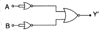
Draw the truth table for all possible values of inputs A and
B. (Comptt. Delhi 2015)
Answer:
(a)
p-n junction diode as full wave
rectifier. A full wave rectifier consists of two diodes and special type of
transformer known as centre tap transformer as shown in the circuit. The
secondary of transformer gives the desired a.c. voltage across A and B.
During the positive half cycle of a.c. input, the diode
D1 is in forward bias and conducts current while D2 is in
reverse biased and does not conduct current. So we get an output voltage across
the load resistor RL. During the negative half cycle of a.c. input,
the diode D1, is in reverse biased and does not conduct current while
diode D2 is in forward biased and conducts current. So we get an
output voltage across the load resistor RL.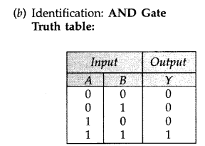
Question 126.
Draw the ‘Energy bands’, diagrams for a
(i) pure
semiconductor
(ii) insulator.
How does the energy band, for a pure
semiconductor, get affected when this semiconductor is doped with
(a) an
acceptor impurity
(b) donor impurity? Hence discuss why the ‘holes’, and the
‘electrons’ respectively, become the ‘majority charge carriers’ in these two
cases? Write the two processes involved in the formation of p-n junction.
(Comptt. All India 2015)
Answer:
‘Energy Band’ diagrams :
Distinguishing features between conductors, semiconductors and insulators :
(i) Insulator. In insulator, the valence band is completely filled. The
conduction band is empty and forbidden energy gap is quite large. So no electron
is able to go from valence band to conduction band even if electric field is
applied. Hence electrical conduction is impossible. The solid/ substance is an
insulator.
(ii) Conductors (Metals). In metals, either the conduction band is partially filled or the conduction and valence band partly overlap each other. If small electric field is applied across the metal, the free electrons start moving in a direction opposite to the direction of electric field. Hence, metal behaves as a conductor.
(iii) Semiconductors. At absolute zero kelvin, the conduction band is empty
and the valence band is filled. The material is insulator at low temperature.
However the energy gap between valence band and conduction band is small. At
room temperature, some valence electrons acquire thermal energy and jump to
conduction band where they can conduct electricity. The holes left behind in
valence band act as a positive charge carrier.
(a) When the semiconductor is doped with an acceptor
impurity, thereby results in an additional energy level a little above the top
of the valence band.
(b) The donor impurity results in an additional energy
level a little below the bottom of the
conduction band.
In the first case, electrons from the valence band, easily jump over to the acceptor lelvel, leaving ‘holes’ behind. Hence, ‘holes’ becomes the majority charge carriers.
In the second case, electrons from the donor level, easily ‘jump over’ to the
conduction band. Hence, electrons become the majority charge carriers. The two
processes involved in the formation of the p-n junction are :
(i)
Diffusion
(ii) Drift
Question 127.
(a) Draw the diagram of the ‘circuit arrangement used for
studying the ‘input’ and ‘output’ characteristics of an n-p-n transistor in its
CE configuration’. Briefly explain how these two types of characteristics are
obtained and draw these characteristics.
(b) ‘Define’ the terms,
(i) Input
resistance
(ii) Output resistance
(iii) Current amplification factor, for
a given transistor. (Comptt. All India 2015)
Answer:
(a)
Common emitter
(CE) transistor characteristics. The transistor is most widely used in the CE
configuration. When a transistor is used in CE configuration, the input is
between the base and emitter and the output is between the collector and
emitter.
The input and the output characteristics of an n-p-n transistor in
CE configuration can be studied by using the circuit as shown in Figure
1.
(i) Input characteristics. The variation of the base current
IB with the base emitter voltage VBE is called the input
characteristic keeping VCE fixed. A curve is plotted between the base
current IB
(ii) Output characteristics. The variation of the collector
current IC with the collector emitter voltage VCE, keeping
the base current IB constant is called output characteristics.
The plot of IC versus VCE for different
fixed values of IB gives one output characteristic. The different
output characteristics for different values of IB is shown in Figure
3.
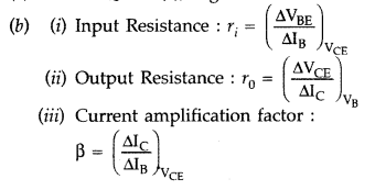
Question 128.
Explain (i) forward biasing and (ii) reverse biasing of a p-n
junction diode.
Answer:
(i) A p-n junction is said to be forward-biased if
its p-type is connected to the positive terminal and its n-type is connected to
the negative terminal of a battery.
(ii) A p-n junction is said to be
reverse-biased if its n-type is connected to the positive terminal and its
p-type is connected to the negative terminal of a battery. The diagrams are as
shown.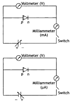
Question 129.
Draw V-l characteristics of a p-n junction diode. Answer the
following questions, giving reasons:
(i) Why is the current under reverse
bias almost independent of the applied potential up to a critical voltage?
(ii) Why does the reverse current show a sudden increase at the critical
voltage? Name any semiconductor device which operates under the reverse bias in
the breakdown region. (CBSEAI 2013)
Answer:
The characteristics are as
shown.
(i) This is because even a small voltage is sufficient to sweep the minority
carriers from one side of the junction to the other side of the junction.
(ii) As the reverse bias voltage is increased, the electric field at the junction becomes significant. When the reverse bias voltage V = Vz critical voltage, then the electric field strength is high enough to pull valence electrons from the host atoms on the p-side which are accelerated to the n-side. These electrons account for the high current observed at the breakdown.
Zener diode operates under the reverse bias in the breakdown region.
Question 130.
Draw the energy band diagrams of (i) n-type and (ii) p-type
semiconductor at temperature T > 0 K.
In the case of n-type Si
semiconductors, the donor energy level is slightly below the bottom of the
conduction band, whereas in p-type semiconductors, the acceptor energy level is
slightly above the top of the valence band. Explain what role do these energy
levels play in conduction and valence bands. (CBSE AI 2015 C)
Answer:
For
energy bands
(i) The energy level diagram is shown below.
(ii) The diagram is shown as
In the energy band diagram of n-type Si semiconductor, the donor energy level
EA is slightly below the bottom Ec of the conduction band and
electrons from this level move into the conduction band with a very small supply
of energy. At room temperature, most of the donor atoms get ionized but very few
(-10-12) atoms of Si get ionized. So the conduction band will have most
electrons coming from the donor impurities.
Similarly, for p-type semiconductors, the acceptor energy level EA is slightly above the top Ev of the valence band. With the very small supply of energy, an electron from the valence band can jump to the level EA and ionize the acceptor negatively. Alternately, we can also say that with a very small supply of energy, the hole from level EA sinks down into the valence band. Electrons rise up and holes fall down when they gain external energy.
Question 131.
Give reasons for the following:
(i) High reverse voltage
does not appear across an LED.
Answer:
It is because the reverse breakdown
voltage of LED is very low, i.e. nearly 5 V.
(ii) Sunlight is not always required for the working of a solar cell.
Answer:
Because solar cells can work with any light whose photon energy is
more than the bandgap energy.
(iii) The electric field, of the junction of a Zener diode, is very high even
for a small reverse bias voltage of about 5 V. (CBSE Delhi 2016C)
Answer:
The heavy doping of p and n sides of the p-n junction makes the depletion region
very thin, hence for a small reverse bias voltage, the electric field is very
high.
Question 132.
State the reason why the photodiode is always operated under
reverse bias. Write the working principle of operation of a photodiode. The
semiconducting material used to fabricate a photodiode has an energy gap of 1.2
eV. Using calculations, show whether it can detect light of a wavelength of 400
nm incident on it. (CBSE Al 2017C)
Answer:
It is easier to observe the
change in the current with the change in the light intensity if a reverse bias
is applied. Thus photodiode is used in the reverse bias mode even when the
current in the forward bias is more the energy gap (Eg) of the
semiconductor, then electron-hole pairs are generated due to the absorption of
photons.
Due to the electric field of the junction, electrons and holes are separated before they recombine. The direction of the electric field is such that electrons reach the n-side and holes reach the p-side. Electrons are collected on the n-side and holes are collected on the p-side giving rise to an emf. When an external load is connected, current flows.
Given λ = 400 nm,
Energy of photon
E = \(\frac{h c}{\lambda}=\frac{6.63
\times 10^{-34} \times 3 \times 10^{8}}{400 \times 10^{-9} \times 1.6 \times
10^{-19}}\) = 3.105 eV
Since the bandgap is lesser than this energy, therefore it will be able to detect the wavelength.
Question 133.
Explain the two processes involved in the formation of a p-n
junction diode. Hence define the term ‘barrier potential’. (CBSE Delhi
2017C)
Answer:
The two processes are
(i) Diffusion and
(ii)
Drift
- Diffusion: The holes diffuse from the p-side to the n-side and electrons diffuse from the n-side to the p-side.
- Drift: The motion of charge carriers due to the applied electric field which results in the drifting of holes along the electric field and of electrons opposite to the electric field.
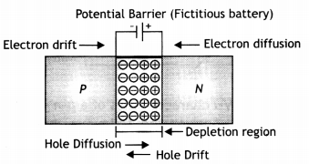
The potential barrier is the fictitious battery that seems to be connected
across the junction with its positive end on the n-type and the negative end on
the p-type.
Question 134.
Explain briefly how a photodiode operates.
Answer:
A
Photodiode is again a special purpose p-n junction diode fabricated with a
transparent window to allow light to fall on the diode. It is operated under
reverse bias. When the photodiode is illuminated with light (photons) with
energy (hv) greater than the energy gap (Eg) of the semiconductor,
then electron-hole pairs are generated due to the absorption of photons. The
diode is fabricated such that the generation of e-h pairs takes place in or near
the depletion region of the diode.
Question 135.
Name the p-n junction diode which emits spontaneous radiation
when forward biased. How do we choose the semiconductor, to be used in these
diodes, if the emitted radiation is to be in the visible region?
Answer:
The p-n junction diode, which emits spontaneous radiation when forward biased,
is the “light-emitting diode” or LED.
The visible tight is from 400 nm to 700 nm and the corresponding energy is between 2.8 eV to 1.8 eV. Therefore, the energy gap of the semiconductor to be used in LED, in order to have the emitted radiation be in the visible region, should be 1.8 eV. Phosphorous doped gallium arsenide and gallium phosphide are two such suitable semiconductors.
Question 136.
The figure shows the V-l characteristic of a semiconductor
diode designed to operate under reverse bias. (CBSE Al 2019)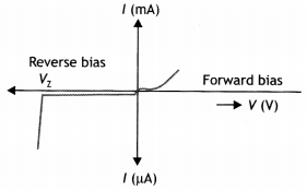
(a) Identify the semiconductor diode used.
Answer:
The diode used is Zener
diode
(b) Draw the circuit diagram to obtain the given characteristics of this
device.
Answer:
The circuit diagram is as shown.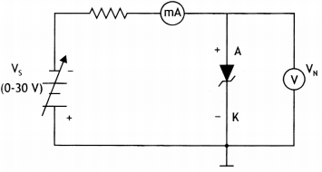
(c) Briefly explain one use of this device.
Answer:
The Zener diode can be
used as a voltage regulator in its breakdown region. The Zener voltage remains
constant even when the current through the Zener diode changes.
Question 137.
With the help of a diagram, show the biasing of a
light-emitting diode (LED). Give its two advantages over conventional
incandescent lamps.
Answer:
The biasing of a light-emitting diode (LED),
has been shown below.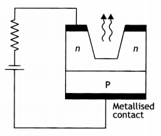
Two main advantages of LED over conventional incandescent lamps are as
follows:
- Low operational voltage and less power consumption.
- Fast action and no warm-up time required.
- The bandwidth of emitted light is 100 A to 500 A or in other words, it is nearly (but not exactly) monochromatic.
- Long life and ruggedness.
- Fast on-off switching capability.
Question 138.
(a) Writetheprincipleofasemiconductor device which is used as
a voltage regulator.
Answer:
(a) Zener diode is used as a voltage
regulator
Principle: It is based on the Principle that when breakdown voltage
V2 takes place, there is a large change in the reverse current even
with the insignificant change in the reverse bias voltage.
(b) With the help of a circuit diagram explain its working.
Answer: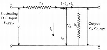
Working: If the reverse voltage across a Zener diode is increased beyond the
breakdown voltage Vz, the current increases sharply and large current
lz flows through the Zener diode and the voltage drop across Rs
increases maintaining the voltage drop across RL at constant value Vo
= Vz.
On the other hand, if we keep the input voltage constant and decrease the load resistance RL, the current across the load will increase. The extra current cannot come from the source because drop-in Rs will not change as the Zener is within its regulating range. The additional load current will pass through the Zener diode and is known as Zener current lz so that the total current (lL + lz) remains constant.
(c) Draw its l-V characteristics. (CBSE 2019C)
Answer:
l-V
Characteristics of Zener diode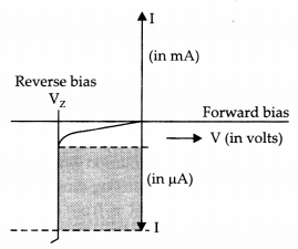
Question 139.
With what considerations in view, a photodiode is fabricated?
State its working with the help of a suitable diagram.
Even though the
current in the forward bias is known to be more than in the reverse bias, yet
the photodiode works in reverse bias. What is the reason? (CBSE Delhi 2015)
Answer:
It is fabricated with a transparent window to allow light to fall on
the diode. It is fabricated such that the generation of e-h pairs takes place in
or near the depletion region of the diode.
When the photodiode is illuminated with light (photons) with energy (hw) greater than the energy gap (Eg) of the semiconductor, then electron-hole pairs are generated due to the absorption of photons. The diode is fabricated such that the generation of e-h pairs takes place in or near the depletion region of the diode. Due to the electric field of the junction, electrons and holes are separated before they recombine.
The direction of the electric field is such that electrons reach the n-side and holes reach the p-side. Electrons are collected on the n-side and holes are collected on the p-side giving rise to an emf. When an external load is connected, current flows. The magnitude of the photocurrent depends on the intensity of incident light (photocurrent is proportional to incident light intensity). The diagram is as shown.
It is easier to observe the change in the current with a change in the light
intensity if a reverse bias is applied. Thus photodiode is used in the reverse
bias mode even when the current in the forward bias is more.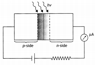
Question 140.
Draw the circuit diagram of a full-wave rectifier and explain
its working. Also, give the input and output waveforms. (CBSE Delhi 2019)
Answer:
The circuit diagram is as shown.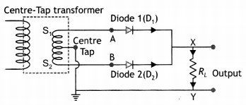
The two ends S1 and S2 of a center-tapped secondary
of a transformer are connected to the P sections of the two diodes D1
and D2 respectively. The n-sections of the two diodes are joined
together and their com¬mon junction is connected to the central tap C of the
secondary winding through a load resistance RL. The input is applied
across the primary and the output is ob¬tained across the load resistance
RL. The arrows show the direction of the current.
Assume that the end A of the secondary is positive during the first half cycle of the supply voltage. This makes diode D1 forward biased and diode D2 reverse biased. Thus diode D1 conducts and an output is obtained across the load RL.
During the second half cycle of the supply voltage, the polarities of the secondary windings reverse. A becomes negative and B becomes positive with respect to the central terminal C. This makes diode D2 forward biased. Hence it conducts and an output is obtained across RL.
The input-output waveforms are as shown.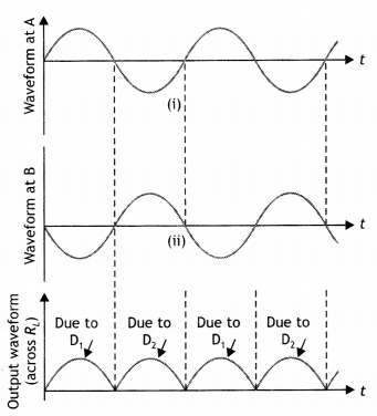
Question 141.
Draw the circuit diagram to show the use of a p-n junction diode
as a half-wave rectifier. Also show the input and the output voltages,
graphically. Explain its working.
Answer:
The diagram is as shown.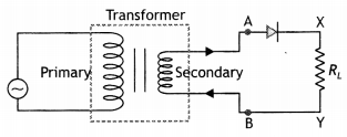
The input and output waveforms are as shown.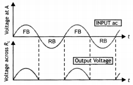
A p-n junction diode is used as a half-wave rectifier. Its work is based on the
fact that the resistance of the p-n junction becomes low when forward biased and
becomes high when reversing biased. These characteristics of a diode are used in
rectification.
Question 142.
Distinguish between conductors, insulators, and
semiconductors on the basis of the band theory of solids.
Answer:
The
diagrams are as shown.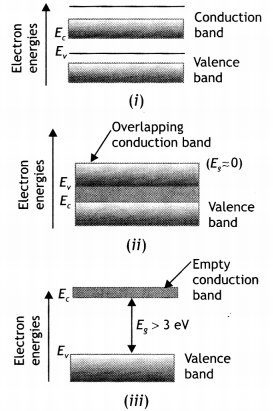
Metals: A distinguishing character of all conductors, including metals, is that
the valence band is partially filled or the conduction and the valence band
overlap. Electrons in states near the top of the filled portion of the band have
many adjacent unoccupied states available, and they can easily gain or lose
small amounts of energy in response to an applied electric field. Therefore
these electrons are mobile and can contribute to electrical and thermal
conductivity. Metallic crystals always have partially filled bands figure
(ii).
Insulators: In the case of insulators, there is a large energy gap of approximately 6 eV depending upon the nature of the crystal. Electrons, however, heated, find it difficult or practically impossible to jump this gap and thus never reach the conduction band. Thus electrical conduction is not possible through an insulator figure (iii).
Semiconductors: There is a separation between the valence band and the conduction band. The energy gap is of the order of 1 eV (0.67 eV for germanium and 1.12 eV for silicon). At absolute zero the electrons cannot gain this energy. But at room temperature, these electrons gain energy and move into the conduction band where they are free to move even under the effect of a weak electric field figure (i).
Question 143.
What is a Zener diode? How is it symbolically represented?
With the help of a circuit diagram, explain the use of the Zener diode as a
voltage stabilizer.
Answer:
It is a special diode made to work only in the
reverse breakdown region.
Symbol: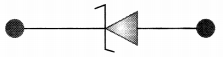
The figure below shows the use of the Zener diode in providing a constant
voltage supply.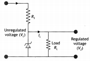
This use of the Zener diode is based on the fact that in the reverse breakdown
(or Zener) region, a very small change in voltage across the Zener diode
produces a very large change in the current through the circuit. If voltage is
increased beyond Zener voltage, the resistance of the Zener diode drops
considerably. Consider that the Zener diode and a resistor R, called dropping
resistor, are connected to a fluctuating voltage supply, such that the Zener
diode is reverse biased.
Whenever voltage across the diode tends to increase, the current through the diode rises out of proportion and causes a sufficient increase in the voltage drop across the dropping resistor. As a result, the output voltage lowers back to the normal value. Similarly, when the voltage across the diode tends to decrease, the current through the diode goes down out of proportion, so that the voltage drop across the dropping resistor is much less and now the output voltage is raised to normal.
Question 144.
Explain briefly with the help of a circuit diagram how V-l
characteristics of a p-n junction diode are obtained in (i) forward bias and
(ii) reverse bias.
Answer:
Forward biased characteristics: A p-n junction
is said to be forward-biased if its p-type is connected to the positive terminal
and its n-type is connected to the negative terminal of a battery shows a
circuit diagram that is used to study the forward characteristics of a p-n
junction. The p-n junction is forward biased. Different readings are taken by
changing the voltage and noting the corresponding milliammeter current.
Practically no current is obtained till the applied voltage becomes greater than the barrier potential. Above the potential barrier voltage, even a small change in potential causes a large change in current.
Reverse biased characteristics: In reverse biased characteristics, instead of a milliammeter, a microammeter is used. The voltage across the p-n junction is increased and the corresponding current is noted.
In the reverse bias, the diode current is very small. As the voltage has
increased the current also increases. At a certain voltage, the current at once
becomes very large. This voltage is called Breakdown voltage or Zener voltage.
At this voltage, a large number of covalent bonds break releasing a large number
of electrons and holes. Hence a large current is obtained. The characteristics
are as shown.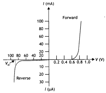
Question 145.
Explain how the heavy doping of the p and n sides of a p-n
junction diode helps in internal field emission (or Zener breakdown), even with
a reverse bias voltage of a few volts only. Draw the general shape of the V-I
characteristics of a Zener diode. Discuss how the nature of these
characteristics led to the use of a Zener diode as a voltage regulator.
Answer:
Consider a p-n junction where both p- and n-sides are heavily doped.
Due to the high dopant densities, the depletion layer junction width is small
and the junction field will be high. Under large reverse bias, the energy bands
near the junction and the junction width decrease. Since the junction width is
< 10-7 m, even a small voltage (say 4 V) may give a field as large
as 4 × 10⁻⁷ Vm-1. The high junction field may strip an
electron from the valence band which can tunnel to the n-side through the thin
depletion layer. Such a mechanism of emission of electrons after a certain
critical field or applied voltage V is termed as internal field emission which
gives rise to a high reverse, current, or breakdown current.
The general shape of the V-l characteristics of a Zener diode is as shown in
the figure.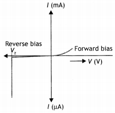
Suppose an unregulated dc input voltage (Vi) is applied to the Zener
diode (whose breakdown voltage is Vz as shown in the figure. If the
applied voltage Vi > Vz, then the Zener diode is in the
breakdown condition. As a result of a wide range of values of load
(RL), the current in the circuit or through the Zener diode may
change but the voltage across it remains unaffected by the load. Thus, the
output voltage across the Zener is a regulated voltage.
Question 146.
(i) Describe briefly with the help of a necessary circuit
diagram, the working principle of a solar cell.
Answer:
Solar Cell: A
solar cell is a junction diode that converts solar energy into electrical
energy. In a solar cell, the n-region is very thin and transparent so that most
of the incident light reaches the junction. The thin region is called the
emitter and the other base. When light is incident on it, it passes through the
crystal onto the junction. The electrons and holes are generated due to light
(with hv > Eg). The electrons are kicked to the n-side
and holes to the p-side due to the electric field of the depletion region. Thus
p-side becomes positive and the n-side becomes negative giving rise to a
photo-voltage. Thus it behaves as a cell.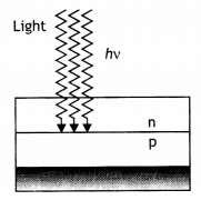
(ii) Why are Si and GaAs preferred materials for solar cells? Explain. (CBSE AI
2011C)
Answer:
Si and GaAs are preferred for solar cell fabrication due to
the fact that their bandgap is ideal. Further, they have high electrical
conductivity and high optical absorption.
Question 147.
Explain, with the help of a circuit diagram, the working of a
photo-diode. Write briefly how it is used to detect optical signals. (CBSE Delhi
2013)
Answer:
When the photodiode is illuminated with light (photons) with
energy (hv) greater than the energy gap (Eg) of the
semiconductor, then – electron-hole pairs are generated due to the absorption of
photons. The diode is fabricated such that the generation of e-h pairs takes
place in or near the depletion region of the diode. Due to the electric field of
the junction, electrons and holes are separated before they recombine. The
direction of the electric field is such that electrons reach the n-side and
holes reach the p-side. Electrons are collected on the n-side and holes are
collected on the p-side giving rise to an emf. When an external load is
connected, current flows.
The magnitude of the photocurrent depends on the intensity of incident light
incident on it. This helps in detecting optical signals.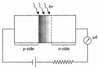
Question 148.
(i) Explain with the help of a diagram, how depletion region and
potential barrier are formed in a junction diode.
(ii) If a small voltage is
applied to a p-n junction diode, how will the barrier potential be affected when
it is (i) forward biased and (ii) reverse biased? (CBSE AI2015)
Answer:
(i) Since there is an excess of electrons in the n-type and excess of holes in
the p-type, on the formation of a p-n junction the electrons from the n-type
diffuse into the p-region, and the holes in the p-type diffuse into the
n-region.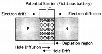
The accumulation of electric charge of opposite polarities in the two regions
across the junction establishes a potential difference between the two regions.
This is called the potential barrier or junction barrier. The potential barrier
developed across the junction opposes the further diffusion of the charge
carriers from p to n and vice versa. There is a region on either side of the
junction where there is a depletion of mobile charges and has only immobile
charges. The region around the junction, which is devoid of any mobile charge
carriers, is called the depletion layer or region.
(ii) (a) In forwarding bias the potential barrier decreases.
(b) In
reverse bias the potential barrier increases.
Question 149.
Write the two processes that take place in the formation of a
p-n junction. Explain with the help of a diagram, the formation of depletion
region and barrier potential in a p-n junction. (CBSE Delhi 2017)
Answer:
- Drift and
- diffusion.
The n-type has an excess of electrons and the p-type has an excess of holes. When a p-n junction has formed the electrons from the n-type diffuse into the p-region and the holes in the p-type diffuse into the n-region. These diffusing electrons and holes combine near the junction. Each combination eliminates an electron and a hole. This results in the n-region near the junction becoming positively charged by losing its electrons and the p-region near the junction becoming negatively charged by losing its holes.
This accumulation of electric charge of opposite polarities in the two
regions across the junction establishes a potential difference between the two
regions. This is called the potential barrier or junction barrier.
The
potential barrier developed across the junction opposes the further diffusion of
the charge carriers from p to n and vice versa. As a result, a region develops
on either side of the junction where there is a depletion of mobile charges and
has only immobile charges. The region around the junction which is devoid of any
mobile charge carriers is called the depletion layer or region.
Question 150.
(i) State briefly the processes involved in the formation of
the p-n junction explaining clearly how the depletion region is formed.
Answer:
As we know that n-type semi-conductor has more concentration of
electrons than that of a hole and a p-type semi-conductor has more concentration
of holes than an electron. Due to the difference in concentration of charge
carriers in the two regions of the p-n junction, the holes diffuse from p-side
to n-side, and electrons diffuse from n-side to p-side. When an electron
diffuses from n to p, it leaves behind it an ionized donor on the n-side. The
ionized donor (+ve charge) is immobile as it is bound by the surrounding atoms.
Therefore, a layer of positive charge is developed on the n-side of the
junction. Similarly, a layer of negative charge is developed on the p-side.
Hence, a space-charge region is formed on either side of the junction, which
has immobile ions and is devoid of any charge carrier, called depletion layer or
depletion region.
The potential barrier is the fictitious battery which seems to be connected
across the junction with its positive end on the n-type and the negative end on
the p-type.
(ii) Using the necessary circuit diagrams, show how the V – l characteristics
of a p-n junction are obtained in
(a) Forward biasing
(b) Reverse
biasing
How these characteristics are made use of in rectification? (CBSE
Delhi 2014)
Answer:
(a) p-n junction diode under forwarding bias: The
p-side is connected to the positive terminal and the n-side to the negative
terminal. Applied voltage drops across the depletion region. Electron in
n-region moves towards the p-n junction and holes in the p-region move towards
the junction. The width of the depletion layer decreases and hence, it offers
less resistance. Diffusion of majority carriers takes place across the junction.
This leads to the forward current.
(b) p-n junction diode under reverse bias: Positive terminal of the battery is connected to the n-side and negative terminal to p-side. Reverse bias supports the potential barrier. Therefore, the barrier height increases and the width of the depletion region also increases. Due to the majority of carriers, there is no conduction across the junction. A few minority carriers across the junction after being accelerated by the high reverse bias voltage. This constitutes a current that flows in opposite direction, which is called reverse current.
For V-l curves
A p-n junction diode is used as a half-wave rectifier. Its work is based on the fact that the resistance of the p-n junction becomes low when forward biased and becomes high when reversing biased. These characteristics of the diode are used in rectification.
Question 151.
(i) Explain with the help of a suitable diagram, the two
processes which occur during the formations of a p-n junction diode. Hence
define the terms (i) depletion region and (ii) potential barrier.
(ii) Draw a
circuit diagram of a p-n junction diode under forwarding bias ‘ and explain its
working. (CBSE 2018C)
Answer:
(i) The two important processes are
diffusion and drift.
Due to the concentration gradient, the electrons diffuse
from the n-side to the p side, and holes diffuse from the n-side to the n
side.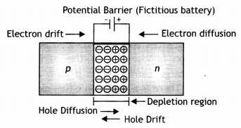
Due to the diffusion, an electric field develops across the junction. Due to the
field, an electron moves from the p-side to the n-side; a hole moves from the
n-side to the p-side. The flow of the charge carriers due to the electric field
is called drift.
(a) Depletion region: It is the space charge region on either side of the
junction that gets depleted of free charges is known as the depletion
region.
(b) Potential Barrier: The potential difference that gets developed
across the junction and opposes the diffusion of charge carriers and brings
about a condition of equilibrium, which is known as the barrier potential.
(ii) The circuit diagram is as shown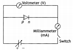
Working:
In the forward bias condition, the direction of the applied voltage
is opposite to the barrier potential. This reduces the width of the depletion
layer as well as the height of the barrier. A current can, therefore, flow
through the circuit. This current increases (non¬linearly) with the increase in
the applied voltage.
Numerical Problems
Question 1.
(i) Three photodiodes D1, D2, and
D3 are made of semiconductors having band gaps of 2.5 eV, 2 eV, and 3
eV respectively. Which of them will not be able to detect light of wavelength
600 nm? (CBSE Delhi 2019)
Answer:
λ = 600 nm
The energy of a photon of
wavelength λ
E = \(\frac{h c}{\lambda}=\frac{6.63 \times 10^{-34} \times 3
\times 10^{8}}{600 \times 10^{-9} \times 1.6 \times 10^{-19}}\) = 2.08 eV
The bandgap energy of diode D2 (= 2eV) is less than the energy of the photon. Hence diode D2 will not be able to detect light of wavelength 600 nm.
(ii) Why photodiodes are required to operate in reverse bias? Explain.
Answer:
A photodiode when operated in reverse bias can measure the fractional
change in minority carrier dominated reverse bias current with greater ease than
when forward biased.
Question 2.
In half-wave rectification, what is the output frequency if
the input frequency is 50 Hz? What is the output frequency of a full-wave
rectifier for the same input frequency? (NCERT)
Answer:
The output
frequency of the half-wave rectifier is the same as the input frequency, while
that of the full-wave rectifier is double that of the input. Therefore the
frequency is 50 Hz for half-wave and 100 Hz for full-wave.
Question 3.
A p-n photodiode is fabricated from a semiconductor with a
bandgap of 2.8 eV. Can it detect a wavelength of 6000 nm? (NCERT)
Answer:
Given λ = 6000 nm,
Energy of photon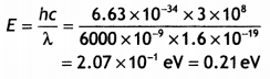
Since the bandwidth is greater than this energy, it will not be able to detect
the wavelength.
Question 4.
Three photodiodes D1, D2, and
D3 are made of semiconductors having band gaps of 2.5 eV, 2 eV, and 3
eV, respectively. Which ones will be able to detect light of wavelength 600 nm?
(NCERT Exemplar)
Answer:
The energy of an incident light photon is given
by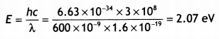
For the incident radiation to be detected by the photodiode, the energy of the
incident radiation photon should be greater than the bandgap. This is true only
for D2. Therefore, only D2 will detect this radiation.
Question 5.
If each diode in the figure has a forward bias resistance of
25 Ω and infinite resistance in reverse bias, what will be the values of the
current l1 l2, l3, and l4? (NCERT
Exemplar)
nswer:
Current l3 is zero as the diode in that branch is
reverse biased.
Resistance in the branches AB and EF is each (125 +25) Ω = 150 Ω
As AB and
EF are identical paraLleL branches, their effective resistance is 150/2 = 75
Ω
Therefore net resistance in the circuit Is
Rnet =75 + 25 = 100 Ω
Therefore current l1 is
l1 = 5/100 = o.05 A
As resistance of branches AB and EF is equal, the current l1 will be equally
shared by the two, hence
l2 = l4 = 0.05/2 = 0.025A
Hence l1 = 0.05 A, l2 = l4 = 0.025 A,
l3 = 0
Question 6.
Assuming the ideal diode, draw the output waveform for the
circuit given in the figure. ExplaIn the waveform. (NCERT Exemplar)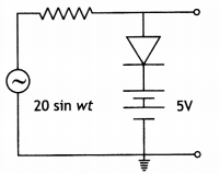
Answer:
When input voltage Will is greater than 5 V, the diode wilt becomes
forward biased and will conduct. When the input is Less than 5 V, the diode will
be reverse biased and will not conduct, i.e. open circuit, hence the output is
as shown.